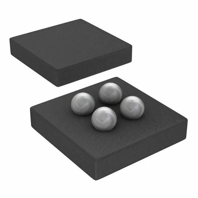
Texas Instruments CSD23202W10

CSD23202W10 P-Channel MOSFET, 12V, 2.2A, 4-DSBGA

MPNCSD23202W10
End of Life

Texas Instruments NexFET P-Channel MOSFET, 12 V drain-to-source, 2.2 A continuous drain at 25 °C, 53 mOhm Rds(on) max at 500 mA and 4.5 V drive, 4-DSBGA 1x1 mm package, -55 to 150 °C junction temperature.

$0.41Ref. price · indicative, final on quote
Packaging4-UFBGA, DSBGA
StockContact for availability
MOQ1 pcs
  • 100% new & originalTraceable channels only — no refurbs, no pulls, no remarked parts.
  • Date & lot codes on quoteStated per line before you commit; label photos on request.
  • MSL-compliant ESD packingMoisture-sealed bags with indicator cards; reels photo-verified.
  • PayPal buyer protectionPay by T/T, PayPal or Payoneer — card payments covered end to end.

Specifications

CSD23202W10 Technical Specifications
ParameterValue
SeriesNexFET™
FET typeP-Channel
Mounting typeSurface Mount
Drain to source voltage12 V
Drive voltage (Max rds on, min rds on)1.5V, 4.5V
Current - continuous drain (Id) @ 25°C2.2A (Ta)
Power dissipation1W (Ta)
Operating temperature-55°C ~ 150°C (TJ)
PackageTape & Reel (TR); Cut Tape (CT)
Vgs-6V
TechnologyMOSFET (Metal Oxide)
Case4-UFBGA, DSBGA
Vgs(th) (Max) @ id900mV @ 250µA
Rds on (Max) @ id, vgs53mOhm @ 500mA, 4.5V
Gate charge (Qg) (Max) @ vgs3.8 nC @ 4.5 V
Input capacitance (Ciss) (Max) @ vds512 pF @ 6 V

Product details

53 mOhm on-resistance at 4.5 V drive

The CSD23202W10: The 53 mOhm Rds(on) at 4.5 V gate drive is the number that sizes the conduction loss — at 500 mA load the voltage drop is under 27 mV, which keeps the dissipation below 14 mW in a typical load-switch application. The 1x1 mm 4-DSBGA package puts the die right at the board surface, so the thermal path is through the solder balls and the PCB copper, not a plastic overmold.

Gate charge and switching speed

Total gate charge is 3.8 nC at 4.5 V, with an input capacitance of 512 pF at 6 V drain bias.

Package and mounting

The 4-DSBGA (1x1 mm) package has four solder balls on a 0.5 mm pitch. No exposed pad, no centre thermal via — the die heat spreads through the BGA balls into the PCB pads. In a field-repair scenario this is not a hand-solder part; you need a hot-air station with a fine nozzle and a stencil for the solder paste. The package marking is minimal — confirm orientation by the pin-1 indicator (a dot or chamfer on the package corner) before placement. Moisture sensitivity level is not listed in the spec, but a 1x1 mm BGA typically runs MSL-1; still, bake at 125 °C for 8 hours if the reel has been open longer than the floor life.

Frequently asked questions

What is the Rds(on) of CSD23202W10?

Maximum on-resistance is 53 mOhm at 500 mA drain current with 4.5 V gate-to-source drive. At the minimum drive voltage of 1.5 V the Rds(on) is higher — the datasheet curve shows it roughly doubles below 2.5 V.

Is CSD23202W10 compatible with 1.8 V logic?

The gate threshold voltage is 900 mV maximum at 250 µA drain current, so a 1.8 V logic output will turn the FET on. But the Rds(on) at 1.8 V drive is not specified — expect it to be significantly higher than the 53 mOhm at 4.5 V. For a load switch pulling 500 mA, the voltage drop at 1.8 V drive could be 100 mV or more, which may be acceptable depending on the load tolerance.

Is CSD23202W10 equivalent to SI2301?

No direct pin-compatible equivalent. The SI2301 is a SOT-23 P-channel MOSFET; the CSD23202W10 is a 4-DSBGA with a completely different footprint and ball map. They share the same function (P-channel load switch) but the package difference means a board respin is required to swap one for the other.