65 mOhm at 10 V — what the on-resistance means for your design
For a 2.2 A load, conduction loss is within the 500 mW package power limit. The 14 nC gate charge at 10 V gives a switching-loss estimate.
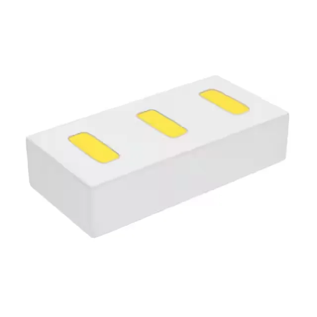
Texas Instruments FemtoFET™ N-Channel MOSFET, 60V Vdss, 2.2A Id, 65mOhm Rds(on) at 10V, 3-PICOSTAR surface-mount package, -55°C to 150°C junction temperature.
| Parameter | Value |
|---|---|
| Series | FemtoFET™ |
| FET type | N-Channel |
| Mounting | Surface Mount |
| Drain to source voltage | 60 V |
| Drive voltage (Max rds on, min rds on) | 4.5V, 10V |
| Current - continuous drain (Id) @ 25°C | 2.2A (Ta) |
| Power dissipation | 500mW (Ta) |
| Operating temperature | -55°C ~ 150°C (TJ) |
| Package | Tape & Reel (TR); Cut Tape (CT) |
| Vgs | ±20V |
| Technology | MOSFET (Metal Oxide) |
| Case | 3-SMD, No Lead |
| Vgs(th) (Max) @ id | 2.2V @ 250µA |
| Rds on (Max) @ id, vgs | 65mOhm @ 1A, 10V |
| Gate charge (Qg) (Max) @ vgs | 14 nC @ 10 V |
| Input capacitance (Ciss) (Max) @ vds | 777 pF @ 30 V |
For a 2.2 A load, conduction loss is within the 500 mW package power limit. The 14 nC gate charge at 10 V gives a switching-loss estimate.
The maximum gate-to-source voltage is ±20 V. The total gate charge at a 10 V gate drive is 14 nC.