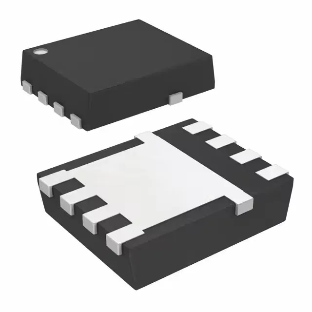
Texas Instruments CSD18532Q5B

CSD18532Q5B NexFET N-Ch 60V 100A MOSFET, 8-VSONP

MPNCSD18532Q5B
End of Life

Texas Instruments NexFET™ N-Channel MOSFET, 60 V drain-source, 100 A continuous drain, 3.2 mOhm Rds(on) at 10 V, 8-PowerTDFN (VSONP 5x6) package, -55°C to 150°C junction temperature.

$2.6Ref. price · indicative, final on quote
Packaging8-PowerTDFN
StockContact for availability
MOQ1 pcs
  • 100% new & originalTraceable channels only — no refurbs, no pulls, no remarked parts.
  • Date & lot codes on quoteStated per line before you commit; label photos on request.
  • MSL-compliant ESD packingMoisture-sealed bags with indicator cards; reels photo-verified.
  • PayPal buyer protectionPay by T/T, PayPal or Payoneer — card payments covered end to end.

Specifications

CSD18532Q5B Technical Specifications
ParameterValue
SeriesNexFET™
FET typeN-Channel
Mounting typeSurface Mount
Drain to source voltage60 V
Drive voltage (Max rds on, min rds on)4.5V, 10V
Current - continuous drain (Id) @ 25°C100A (Ta)
Power dissipation3.2W (Ta), 156W (Tc)
Operating temperature-55°C ~ 150°C (TJ)
PackageTape & Reel (TR); Cut Tape (CT)
Vgs±20V
TechnologyMOSFET (Metal Oxide)
Case8-PowerTDFN
Vgs(th) (Max) @ id2.2V @ 250µA
Rds on (Max) @ id, vgs3.2mOhm @ 25A, 10V
Gate charge (Qg) (Max) @ vgs58 nC @ 10 V
Input capacitance (Ciss) (Max) @ vds5070 pF @ 30 V

Product details

What this 60 V NexFET delivers

The Texas Instruments CSD18532Q5B is a 60 V N-channel NexFET power MOSFET rated for 100 A continuous drain current at 25°C case temperature. Its 3.2 mOhm maximum on-resistance at 10 V gate drive keeps conduction losses low in high-current switching stages — buck converters, motor-drive half-bridges, and battery-management disconnect switches. The package with exposed drain pad pulls heat into the PCB copper plane; the 156 W power dissipation at the case is the thermal limit when the pad is properly soldered to a thermal via array. The -55°C to 150°C junction temperature range covers automotive under-hood and industrial high-ambient environments without derating at the hot end.

Gate charge and switching speed

Total gate charge is 58 nC at 10 V. Input capacitance is 5070 pF at 30 V drain bias.

Package and mounting

The 8-PowerTDFN (VSONP 5x6) has a 5 mm × 6 mm footprint with a large exposed drain pad on the bottom. The PCB land pattern should match the pad dimensions in the datasheet layout recommendation.

Lifecycle and sourcing

No end-of-life notice or last-time-buy window is in effect. For dual-sourcing resilience, verify the Rds(on) and gate-charge differences against your loss budget before substituting.

Frequently asked questions

What is the maximum drain current of CSD18532Q5B?

The continuous drain current at 25°C case temperature is 100 A. This is the package-limited rating when the drain pad is soldered to a sufficient copper area; derate linearly above 25°C per the thermal curve in the datasheet.

What is the Rds(on) of CSD18532Q5B?

Maximum on-resistance is 3.2 mOhm at 25 A drain current and 10 V gate drive. At 4.5 V drive the Rds(on) is higher — the 10 V drive is recommended for full conduction loss performance.

Is CSD18532Q5B a direct replacement for CSD18533Q5B?

The CSD18533Q5B is a pin-compatible sibling in the same NexFET family and same 8-VSONP package. Check the Rds(on) and gate-charge specs against your application — the two parts differ in those parameters, so confirm your loss budget allows the swap.

What is the typical gate charge of CSD18532Q5B?

Maximum total gate charge is 58 nC at 10 V gate-source voltage. This is the charge the gate driver must deliver to switch the FET on; a driver with 2 A peak current handles it cleanly.