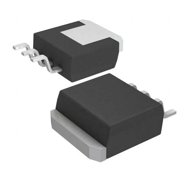
Texas Instruments CSD18510KTTT

CSD18510KTTT NexFET N-Channel MOSFET, 40V 274A DDPAK

MPNCSD18510KTTT
End of Life

Texas Instruments NexFET™ N-Channel MOSFET, 40V Vds, 274A Id, 2.6mOhm Rds(on) at 10V, DDPAK/TO-263-3 surface mount, -55°C to 175°C junction temperature.

$2.8Ref. price · indicative, final on quote
PackagingTO-263-4, D²Pak (3 Leads + Tab), TO-263AA
StockContact for availability
MOQ1 pcs
  • 100% new & originalTraceable channels only — no refurbs, no pulls, no remarked parts.
  • Date & lot codes on quoteStated per line before you commit; label photos on request.
  • MSL-compliant ESD packingMoisture-sealed bags with indicator cards; reels photo-verified.
  • PayPal buyer protectionPay by T/T, PayPal or Payoneer — card payments covered end to end.

Specifications

CSD18510KTTT Technical Specifications
ParameterValue
SeriesNexFET™
FET typeN-Channel
Mounting typeSurface Mount
Drain to source voltage40 V
Drive voltage (Max rds on, min rds on)4.5V, 10V
Current - continuous drain (Id) @ 25°C274A (Tc)
Power dissipation250W (Ta)
Operating temperature-55°C ~ 175°C (TJ)
PackageTape & Reel (TR); Cut Tape (CT)
Vgs±20V
TechnologyMOSFET (Metal Oxide)
CaseTO-263-4, D²Pak (3 Leads + Tab), TO-263AA
Vgs(th) (Max) @ id2.3V @ 250µA
Rds on (Max) @ id, vgs2.6mOhm @ 100A, 10V
Gate charge (Qg) (Max) @ vgs132 nC @ 10 V
Input capacitance (Ciss) (Max) @ vds11400 pF @ 15 V

Product details

What this part is and where it fits

The Texas Instruments CSD18510KTTT is a 40 V N-channel NexFET power MOSFET in a DDPAK/TO-263-3 surface-mount package. It delivers a continuous drain current of 274 A at case temperature, with a maximum Rds(on) of 2.6 mOhm at 10 V gate drive. This combination of low on-resistance and high current capability makes it suited for high-efficiency power switching in motor drives, DC-DC converters, and battery protection circuits. The -55°C to 175°C junction temperature range supports deployment in automotive under-hood and industrial environments where thermal cycling is a factor.

Key ratings and what they mean for the BOM

The 40 V drain-source voltage (Vdss) sets the maximum bus voltage this MOSFET can block. Gate charge (Qg) of 132 nC at 10 V means the gate driver must supply this charge each switching cycle.

Package and mounting

The DDPAK/TO-263-3 (D²Pak) is a surface-mount package with a large exposed drain tab for heat sinking. The tab is electrically connected to the drain, so the PCB copper pour must be sized for both thermal dissipation and electrical clearance. The three-lead plus tab footprint is standard for high-current TO-263 devices; verify the land pattern matches the supplier device package (DDPAK/TO-263-3) before layout.

Lifecycle and sourcing

It is ROHS3 compliant.

Frequently asked questions

CSD18510KTTT datasheet pdf download

Design engineers need to validate electrical parameters and package details before finalizing the part in a circuit.

CSD18510KTTT price and stock

Sourcing buyers must confirm cost and immediate availability to fill production BOM lines quickly.

Where to buy CSD18510KTTT

Transactional intent buyers are ready to purchase and need trusted distributor links to place order.

CSD18510KTTT replacement or equivalent

Maintenance techs and brokers need alternatives if the part is obsolete or out of stock.

Is CSD18510KTTT obsolete?

Lifecycle status determines whether continued production and long-term support are available for existing designs.

CSD18510KTTT pinout and footprint

Design engineers require mechanical dimensions and pin assignments for PCB layout and compatibility checking.