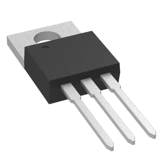
40 V, 100 A, 4.5 mOhm — the power path numbers
The 36 nC total gate charge at 10 V keeps switching losses moderate for a 100 A device; a standard gate driver with 1 A peak output can drive it into the 50–100 kHz range without excessive driver heating.
Gate drive voltage — 10 V for rated Rds(on), 4.5 V for light loads
The datasheet specifies Rds(on) at Vgs = 10 V, which is the standard drive level for this class of NexFET. The drive voltage range listed is 4.5 V to 10 V, meaning the FET will turn on with a 5 V logic-level gate signal, but the on-resistance will be higher than the 4.5 mOhm headline figure — expect roughly double at 4.5 V based on the typical Vgs vs Rds(on) curve for this generation of NexFET trench technology. For applications where the gate drive is limited to 5 V, the 2.3 V maximum threshold at 250 µA ensures the device is fully enhanced, but the higher Rds(on) must be factored into the thermal budget.
Through-hole TO-220-3 — board and thermal interface
The mounting hole accommodates an M3 screw and a TO-220 heatsink clip or spring. For motor-drive or power-supply layouts, the tab is at drain potential, so the heatsink must be electrically isolated or the system must tolerate the tab voltage.
The NexFET series is a mature TI trench MOSFET family with multiple Rds(on) and voltage variants sharing the same TO-220 footprint, so a second-source or alternate density option is straightforward if supply tightens.