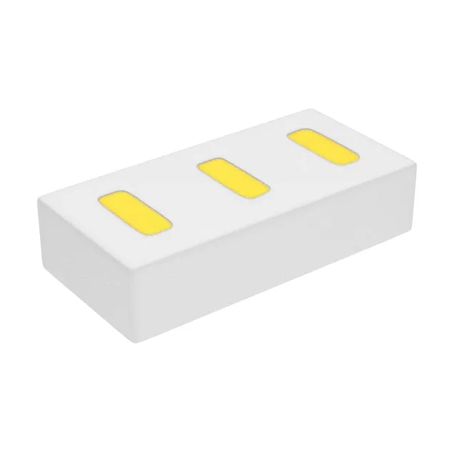
The CSD17585F5T: ROHS3 compliant per, so it clears EU regulatory gates without an exemption review.
The 5.9 A continuous drain rating at 25 °C case temperature drops with board copper and ambient; in a typical 1 oz, 1-inch² pad on FR4, expect about 3.5 A practical limit before the 500 mW package dissipation is reached. At 5.9 A the I²R loss is under 1 W — the package can't sink that continuously, so the part is sized for pulsed or moderate-load duty where the thermal time constant of the board averages the dissipation.
3-PICOSTAR footprint — what it costs in assembly and thermal management
The 3-PICOSTAR is a 3-lead no-lead package roughly 1.0 mm × 0.6 mm — smaller than an SOT-23 by a factor of four. The drain is the large backside pad; the source and gate are the two small pads on the same face. Solder paste stencil aperture for the drain pad needs to be about 70 % of the pad area to avoid solder balling under reflow. The thermal path is almost entirely through the drain pad to the board copper — no lead frame to wick heat. A 0.6 mm pitch means the reflow profile must stay below 260 °C peak with a ramp rate under 3 °C/s to avoid tombstoning the tiny gate pad.
Gate charge and switching — 5.1 nC at 10 V
Total gate charge Qg is 5.1 nC at Vgs = 10 V. A 3.3 V GPIO from a microcontroller can drive the gate directly for low-frequency switching — the 380 pF input capacitance at 15 V drain bias means the gate rise time is about 1.3 µs with a 10 mA drive. For switching above 100 kHz, a dedicated gate driver with 2 A peak current cuts the rise time to under 10 ns.