The drive voltage range (4.5 V to 10 V for rated Rds(on)) allows logic-level drive from a 5 V rail, though the lowest on-resistance is achieved at 10 V.
Thermal reality behind the 100 A rating
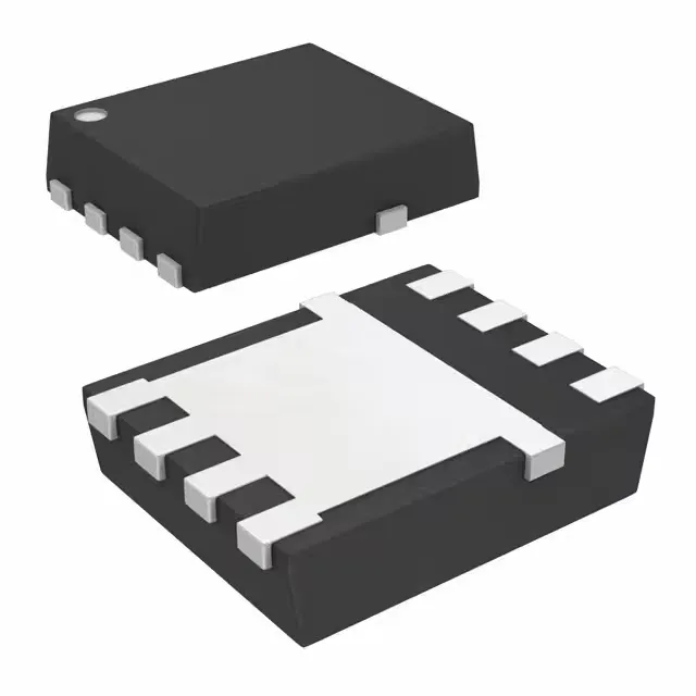
The 100 A continuous drain rating is at 25 °C case temperature, but the maximum power dissipation is 3.2 W at 25 °C ambient. In practice, the continuous current is limited by the board's ability to sink heat from the 8-VSON-CLIP (5x6 mm) package.
The 8-PowerTDFN (5x6 VSON-CLIP) package has an exposed drain pad on the bottom. The PCB layout must use multiple vias under the pad to conduct heat to inner copper planes — the datasheet's recommended footprint is non-negotiable for achieving the rated current. Surface-mount assembly with a standard reflow profile works; the package is ROHS3 compliant.
It is quoted to order against BOM quantities through independent distribution.