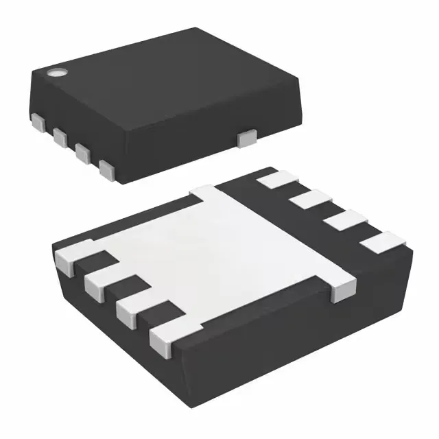
Texas Instruments CSD17552Q5A

CSD17552Q5A NexFET N-Ch 30V MOSFET, 6.2mOhm Rds(on), 8-VSONP

MPNCSD17552Q5A
End of Life

Texas Instruments NexFET™ N-Channel MOSFET, CSD17552Q5A, 30V Vdss, 17A (Ta) / 60A (Tc), 6.2mOhm Rds(on) at 15A/10V, 12nC Qg at 4.5V, -55°C to 150°C, 8-PowerTDFN / 8-VSONP (5x6).

$1.09Ref. price · indicative, final on quote
Packaging8-PowerTDFN
StockContact for availability
MOQ1 pcs
  • 100% new & originalTraceable channels only — no refurbs, no pulls, no remarked parts.
  • Date & lot codes on quoteStated per line before you commit; label photos on request.
  • MSL-compliant ESD packingMoisture-sealed bags with indicator cards; reels photo-verified.
  • PayPal buyer protectionPay by T/T, PayPal or Payoneer — card payments covered end to end.

Specifications

CSD17552Q5A Technical Specifications
ParameterValue
SeriesNexFET™
FET typeN-Channel
Mounting typeSurface Mount
Drain to source voltage30 V
Drive voltage (Max rds on, min rds on)4.5V, 10V
Current - continuous drain (Id) @ 25°C17A (Ta), 60A (Tc)
Power dissipation3W (Ta)
Operating temperature-55°C ~ 150°C (TJ)
PackageTape & Reel (TR); Cut Tape (CT)
Vgs±20V
TechnologyMOSFET (Metal Oxide)
Case8-PowerTDFN
Vgs(th) (Max) @ id1.9V @ 250µA
Rds on (Max) @ id, vgs6.2mOhm @ 15A, 10V
Gate charge (Qg) (Max) @ vgs12 nC @ 4.5 V
Input capacitance (Ciss) (Max) @ vds2050 pF @ 15 V

Product details

6.2 mOhm at 15 A, 10 V drive — the conduction loss floor

The Texas Instruments CSD17552Q5A is a NexFET series N-channel MOSFET in an 8-PowerTDFN package, rated for 30 V drain-to-source. The on-resistance of 6.2 mOhm max at 15 A with 10 V gate drive sets the conduction loss for a given load current.

12 nC gate charge — logic-level drive ready

Gate charge is 12 nC max at 4.5 V, which means a 5 V logic-level gate driver can switch this FET without a separate gate-drive boost stage. The drive voltage range of 4.5 V to 10 V for achieving the rated Rds(on) covers both 5 V logic and 10 V gate-drive rails. Input capacitance is 2050 pF at 15 V drain bias — modest enough that the gate driver's peak current capability sets the switching speed, not the FET's input charge.

The 3 W power dissipation at ambient (Ta) is the limit with minimal copper; the actual thermal capability depends on the PCB's copper area under the exposed pad.

Active production, ROHS3 compliant

It is ROHS3 compliant, with no lead or restricted substances above the threshold.

Frequently asked questions

Is CSD17552Q5A RoHS and lead-free compliant?

Yes, the CSD17552Q5A is listed as ROHS3 compliant, meaning it meets the EU RoHS directive with no restricted substances above the threshold.

What is the Rds(on) of CSD17552Q5A?

The maximum on-resistance is 6.2 mOhm at 15 A drain current with 10 V gate drive. This is the conduction loss figure to use for thermal budgeting at the operating current.

What is the gate charge specification for CSD17552Q5A?

Maximum gate charge is 12 nC at 4.5 V gate voltage. This low Qg allows efficient switching from a 5 V logic-level gate driver without additional gate-drive circuitry.