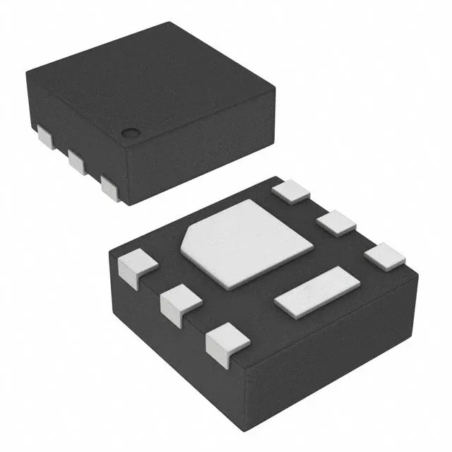
Texas Instruments CSD17313Q2T

CSD17313Q2T NexFET N-Ch MOSFET, 30V 5A, 30mOhm

MPNCSD17313Q2T
End of Life

Texas Instruments NexFET™ N-Channel MOSFET, 30 V drain-source, 5 A continuous drain, 30 mOhm Rds(on) at 4 A / 8 V, 2.7 nC gate charge, 6-WSON (2x2 mm) exposed pad package, -55°C to 150°C junction temperature.

$1.2Ref. price · indicative, final on quote
Packaging6-WDFN Exposed Pad
StockContact for availability
MOQ1 pcs
  • 100% new & originalTraceable channels only — no refurbs, no pulls, no remarked parts.
  • Date & lot codes on quoteStated per line before you commit; label photos on request.
  • MSL-compliant ESD packingMoisture-sealed bags with indicator cards; reels photo-verified.
  • PayPal buyer protectionPay by T/T, PayPal or Payoneer — card payments covered end to end.

Specifications

CSD17313Q2T Technical Specifications
ParameterValue
SeriesNexFET™
FET typeN-Channel
Mounting typeSurface Mount
Drain to source voltage30 V
Drive voltage (Max rds on, min rds on)3V, 8V
Current - continuous drain (Id) @ 25°C5A (Ta)
Power dissipation2.4W (Ta), 17W (Tc)
Operating temperature-55°C ~ 150°C (TJ)
PackageTape & Reel (TR); Cut Tape (CT)
Vgs+10V, -8V
TechnologyMOSFET (Metal Oxide)
Case6-WDFN Exposed Pad
Vgs(th) (Max) @ id1.8V @ 250µA
Rds on (Max) @ id, vgs30mOhm @ 4A, 8V
Gate charge (Qg) (Max) @ vgs2.7 nC @ 4.5 V
Input capacitance (Ciss) (Max) @ vds340 pF @ 15 V

Product details

30 V, 5 A NexFET in a 2x2 mm WSON

The CSD17313Q2T: Key switching characteristics include a maximum Rds(on) of 30 mOhm at 4 A with an 8 V gate drive, and a gate charge of 2.7 nC at 4.5 V. The low gate charge keeps driver losses minimal in high-frequency dc-dc converters, while the 340 pF input capacitance at 15 V Vds gives the designer a clean number for gate-drive sizing and switching-loss estimation.

Active, ROHS3, surface-mount

It is ROHS3 compliant. Mounting is surface-mount only, with a 6-WSON exposed pad case that requires a thermal land on the PCB for the 2.4 W (Ta) / 17 W (Tc) power dissipation capability.

Frequently asked questions

What is the closest pin-compatible alternative to CSD17313Q2T in this component family?

Within the NexFET series, TI offers several 30 V N-channel parts in similar 2x2 mm WSON packages. The exact pin-compatible equivalent depends on the Rds(on) and gate-charge target for your design; check the NexFET parametric table for a like-for-like swap. No single alternative is declared as an official second source in the available documentation.

Can CSD17313Q2T be used for high-frequency switching?

Yes — the 2.7 nC gate charge at 4.5 V and 340 pF input capacitance are low enough for switching frequencies in the hundreds of kHz range common in dc-dc converters. The 30 mOhm Rds(on) keeps conduction losses manageable at those frequencies, provided the PCB thermal land handles the dissipation.

Is CSD17313Q2T RoHS compliant?

Yes, the part is ROHS3 compliant.

What is the recommended footprint for CSD17313Q2T?

The supplier device package is 6-WSON (2x2 mm) with an exposed pad. The exact land pattern and thermal-via layout are in the TI datasheet — the exposed pad must be soldered to a copper plane for the 17 W (Tc) power dissipation rating to hold.