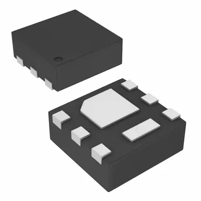
The CSD17313Q2: The 6-WSON exposed-pad package (2x2 mm body) is a surface-mount design. The small footprint suits it for dense layouts, but the pad pattern and via array under the pad are critical for thermal performance — a standard two-layer board with a few thermal vias will handle the 2.3 W, but verify the junction temperature stays below 150°C under worst-case load.
It is ROHS3 compliant.