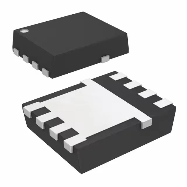
Low-side switch and synchronous rectifier choice
The Texas Instruments CSD17306Q5A is a NexFET™ N-channel MOSFET in an 8-VSONP (5x6) package, rated for 30 V drain-source and 100 A continuous drain at the case. The 3.7 mOhm maximum Rds(on) at 22 A and 8 V gate drive is the spec that sets its conduction loss floor — at 22 A the dissipation in the channel is under 1.8 W, which keeps the junction temperature rise manageable in a 3.2 W ambient-rated package.
Total gate charge is 15.3 nC at 4.5 V, which means a 3.3 V logic-level driver can fully enhance the channel without a separate gate-drive rail. The 2170 pF input capacitance at 15 V Vds gives a rough Miller plateau charge that a typical 1 A gate driver can push through in under 20 ns — fast enough for a 500 kHz switching regulator without excessive cross-conduction.
Temperature range and derating
The 3.2 W power dissipation at 25°C ambient is the limit when the bottom-side copper pad is soldered to the board — above 25°C the allowable dissipation derates linearly. For a 100 A load at the case, the Rds(on) roughly doubles at 125°C junction, so the actual conduction loss at high temperature is about double the 25°C figure.
The leads are on a single row along two sides — the part is not a standard SOIC footprint, so the PCB layout needs the specific VSONP land pattern. The supplier device package is 8-VSONP (5x6), which is the same body size as the industry-standard 5x6 mm DFN.