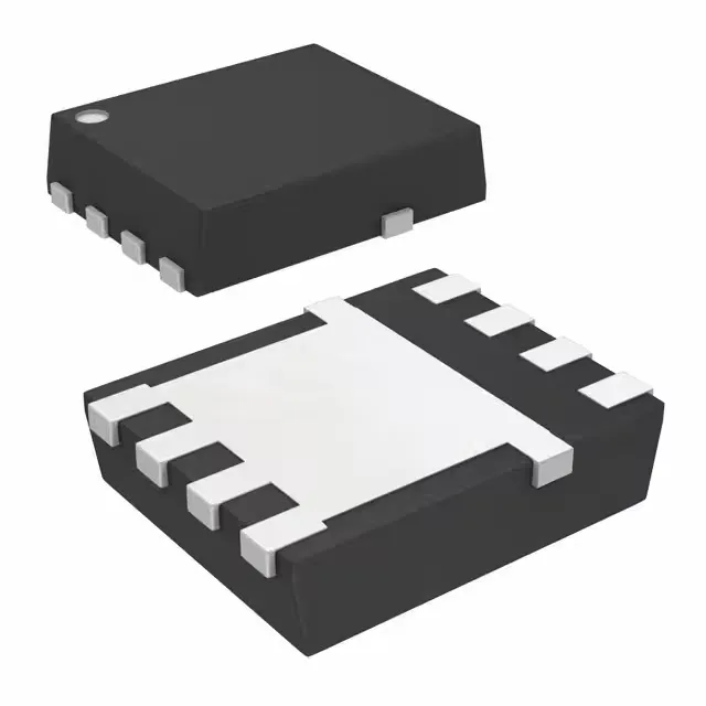
Texas Instruments CSD16414Q5

CSD16414Q5 NexFET N-Channel MOSFET, 25 V, 1.9 mOhm

MPNCSD16414Q5
End of Life

Texas Instruments NexFET™ N-Channel MOSFET, 25 V Vds, 34 A (Ta) / 100 A (Tc), 1.9 mOhm Rds(on) at 10 V, 8-PowerTDFN / 8-VSON-CLIP package, -55 to 150 °C.

$2.09Ref. price · indicative, final on quote
Packaging8-PowerTDFN
StockContact for availability
MOQ1 pcs
  • 100% new & originalTraceable channels only — no refurbs, no pulls, no remarked parts.
  • Date & lot codes on quoteStated per line before you commit; label photos on request.
  • MSL-compliant ESD packingMoisture-sealed bags with indicator cards; reels photo-verified.
  • PayPal buyer protectionPay by T/T, PayPal or Payoneer — card payments covered end to end.

Specifications

CSD16414Q5 Technical Specifications
ParameterValue
SeriesNexFET™
FET typeN-Channel
Mounting typeSurface Mount
Drain to source voltage25 V
Drive voltage (Max rds on, min rds on)4.5V, 10V
Current - continuous drain (Id) @ 25°C34A (Ta), 100A (Tc)
Power dissipation3.2W (Ta)
Operating temperature-55°C ~ 150°C (TJ)
PackageTape & Reel (TR); Cut Tape (CT)
Vgs+16V, -12V
TechnologyMOSFET (Metal Oxide)
Case8-PowerTDFN
Vgs(th) (Max) @ id2V @ 250µA
Rds on (Max) @ id, vgs1.9mOhm @ 30A, 10V
Gate charge (Qg) (Max) @ vgs21 nC @ 4.5 V
Input capacitance (Ciss) (Max) @ vds3650 pF @ 12.5 V

Product details

NexFET N-channel — 25 V, 1.9 mOhm in a 5x6 mm clip package

The Texas Instruments CSD16414Q5 is a NexFET N-channel MOSFET rated for 25 V drain-source, with an on-resistance of 1.9 mOhm maximum at 30 A and 10 V gate drive. It carries a continuous drain current of 34 A at 25 °C ambient (Ta) and 100 A at case temperature (Tc), making it a fit for 12 V input synchronous buck converters, OR-ing diodes, and load switches where board space is tight. The package measures 5x6 mm and uses a copper clip construction. Gate charge is 21 nC at 4.5 V.

Rds(on) and gate charge — what they mean for the switching loop

At 1.9 mOhm max with 10 V gate drive, the CSD16414Q5 delivers a conduction loss of roughly 1.9 W at 30 A — acceptable for a 3.2 W package dissipation limit when the board copper and airflow are adequate. The 21 nC Qg at 4.5 V means the driver sees a moderate capacitive load; a standard 2 A gate driver can switch it in under 30 ns, supporting the high-frequency-switching use case a buyer may be evaluating. Input capacitance is 3650 pF at 12.5 V Vds.

Temperature range and package — deployment context

Junction temperature range is -55 to 150 °C. The package has an exposed pad for thermal relief.

Lifecycle and sourcing posture

The CSD16414Q5 is listed as Active with ROHS3 compliance. No end-of-life notice or last-time-buy schedule has been issued.

Frequently asked questions

What is the Rds(on) of CSD16414Q5?

The maximum Rds(on) is 1.9 mOhm at a drain current of 30 A with a 10 V gate drive. The typical value will be lower; the datasheet provides the typical curve.

What is the equivalent of CSD16414Q5?

No pin-compatible second source is listed in the official cross-reference. For a dual-source option, evaluate other NexFET parts in the 8-VSON-CLIP package with similar Vds and Rds(on) ratings, but confirm pinout and gate drive compatibility from the respective datasheets.

Is CSD16414Q5 suitable for high frequency switching?

Yes, the 21 nC gate charge at 4.5 V and clip-package inductance make it suitable for switching frequencies up to about 1 MHz in a well-laid-out synchronous buck. The 3650 pF input capacitance requires a low-impedance gate drive to avoid excessive switching loss at the high end of that range.