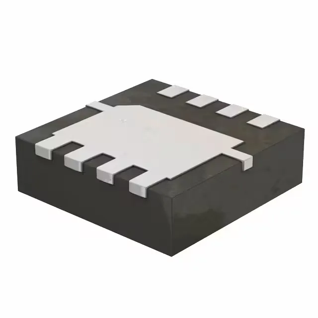
The CSD16406Q3 is a Texas Instruments NexFET N-channel MOSFET rated for a 25 V drain-source voltage and a continuous drain current of 19 A at the ambient temperature case (Ta), or 60 A when the case temperature (Tc) is held at 25 °C. The 8-VSON-CLIP package (3.3x3.3 mm) uses a copper clip construction that lowers package resistance and inductance compared to conventional wire-bonded SO-8 devices, which matters for high-frequency switching loops.
Rds(on), gate charge, and driving from logic-level voltages
Maximum on-resistance is 5.3 mOhm at a 20 A drain current with 10 V gate drive — the 4.5 V and 10 V drive voltage levels listed for minimum and maximum Rds(on) mean this MOSFET can be turned on hard with either standard logic-level (5 V) or full 10 V gate drive. The 8.1 nC gate charge at 4.5 V is low enough that a microcontroller GPIO with a series resistor can switch it at moderate frequencies (tens of kHz) without a dedicated gate driver, provided the GPIO source current is adequate to charge the 1100 pF input capacitance within the desired switching time.
Thermal limits and the 19 A vs 60 A current rating
The 2.7 W maximum power dissipation at ambient (Ta) is the limiting factor for a board-level design without heatsinking: at 19 A continuous, the conduction loss alone (I² × Rds(on)) already exceeds 1.9 W at 25 °C junction, leaving little margin. The 60 A case-temperature rating assumes the MOSFET is mounted on a heatsink or PCB copper area that holds the case at 25 °C — a realistic scenario only with a large thermal pad and forced airflow. Derate above 25 °C following the typical Rds(on) temperature coefficient (roughly 0.4 %/°C).
Active production status and sourcing
It is ROHS3 compliant.