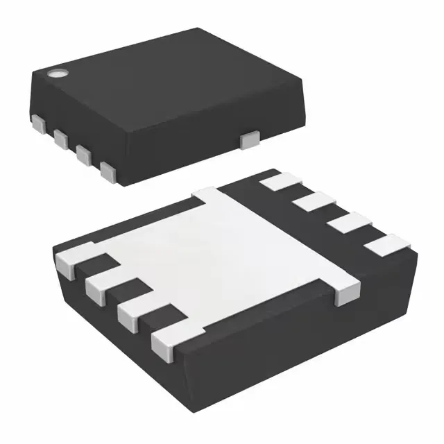
Texas Instruments CSD16401Q5

CSD16401Q5 NexFET N-Channel MOSFET, 25V, 1.6 mOhm

MPNCSD16401Q5
End of Life

Texas Instruments NexFET™ N-Channel MOSFET, 25V Vdss, 1.6mOhm Rds(on) at 10V, 38A (Ta) / 100A (Tc) continuous drain, 29nC gate charge, 8-VSON-CLIP (5x6) package, -55°C to 150°C junction temperature.

$2.53Ref. price · indicative, final on quote
Packaging8-PowerTDFN
StockContact for availability
MOQ1 pcs
  • 100% new & originalTraceable channels only — no refurbs, no pulls, no remarked parts.
  • Date & lot codes on quoteStated per line before you commit; label photos on request.
  • MSL-compliant ESD packingMoisture-sealed bags with indicator cards; reels photo-verified.
  • PayPal buyer protectionPay by T/T, PayPal or Payoneer — card payments covered end to end.

Specifications

CSD16401Q5 Technical Specifications
ParameterValue
SeriesNexFET™
FET typeN-Channel
Mounting typeSurface Mount
Drain to source voltage25 V
Drive voltage (Max rds on, min rds on)4.5V, 10V
Current - continuous drain (Id) @ 25°C38A (Ta), 100A (Tc)
Power dissipation3.1W (Ta)
Operating temperature-55°C ~ 150°C (TJ)
PackageTape & Reel (TR); Cut Tape (CT)
Vgs+16V, -12V
TechnologyMOSFET (Metal Oxide)
Case8-PowerTDFN
Vgs(th) (Max) @ id1.9V @ 250µA
Rds on (Max) @ id, vgs1.6mOhm @ 40A, 10V
Gate charge (Qg) (Max) @ vgs29 nC @ 4.5 V
Input capacitance (Ciss) (Max) @ vds4100 pF @ 12.5 V

Product details

NexFET N-channel for low-voltage power stages

The Texas Instruments CSD16401Q5 is a 25 V N-channel NexFET MOSFET in an 8-VSON-CLIP (5x6) package, rated for 38 A continuous drain at 25°C ambient and 100 A at case temperature.

Gate charge and switching speed

Total gate charge is 29 nC at 4.5 V drive, which keeps the gate-drive energy per cycle low. In a 500 kHz converter the average gate-drive current is about 14.5 mA — well within the capability of a standard MOSFET driver IC. The input capacitance of 4100 pF at 12.5 V drain-source means the driver sees a moderate capacitive load; rise and fall times are determined by the driver's source/sink current and the external gate resistor.

Thermal and package reality

The 3.1 W power dissipation at 25°C ambient (Ta) is the limit when the device is mounted on a standard FR-4 board with minimal copper. The 100 A drain current at case temperature (Tc) assumes the bottom-side exposed pad is soldered to a large copper pour and the junction stays below 150°C. The VSON-CLIP package uses a copper clip over the die instead of bond wires, which reduces package resistance and improves heat spreading into the PCB — a real advantage over a conventional DFN in the same footprint.

Frequently asked questions

Is CSD16401Q5 RoHS compliant?

Yes, the CSD16401Q5 is ROHS3 compliant, meaning it meets the latest EU RoHS directive with no exemptions for lead, mercury, cadmium, or other restricted substances.

What is the gate charge of CSD16401Q5?

The total gate charge (Qg) is 29 nC at 4.5 V gate-source voltage. This low value allows fast switching with a modest gate-drive current, making the part suitable for high-frequency DC-DC converters.