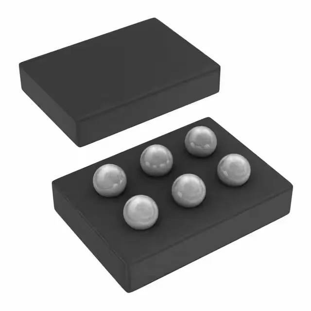
Texas Instruments CSD13306W

Texas Instruments CSD13306W NexFET N-Channel MOSFET

MPNCSD13306W
End of Life

Texas Instruments NexFET™ N-Channel MOSFET, 12 V drain-source, 3.5 A continuous drain, 10.2 mOhm Rds(on) at 4.5 V, 6-DSBGA (1x1.5) package, -55°C to 150°C junction temperature.

$0.54Ref. price · indicative, final on quote
Packaging6-UFBGA, DSBGA
StockContact for availability
MOQ1 pcs
  • 100% new & originalTraceable channels only — no refurbs, no pulls, no remarked parts.
  • Date & lot codes on quoteStated per line before you commit; label photos on request.
  • MSL-compliant ESD packingMoisture-sealed bags with indicator cards; reels photo-verified.
  • PayPal buyer protectionPay by T/T, PayPal or Payoneer — card payments covered end to end.

Specifications

CSD13306W Technical Specifications
ParameterValue
SeriesNexFET™
FET typeN-Channel
Mounting typeSurface Mount
Drain to source voltage12 V
Drive voltage (Max rds on, min rds on)2.5V, 4.5V
Current - continuous drain (Id) @ 25°C3.5A (Ta)
Power dissipation1.9W (Ta)
Operating temperature-55°C ~ 150°C (TJ)
PackageTape & Reel (TR); Cut Tape (CT)
Vgs±10V
TechnologyMOSFET (Metal Oxide)
Case6-UFBGA, DSBGA
Vgs(th) (Max) @ id1.3V @ 250µA
Rds on (Max) @ id, vgs10.2mOhm @ 1.5A, 4.5V
Gate charge (Qg) (Max) @ vgs11.2 nC @ 4.5 V
Input capacitance (Ciss) (Max) @ vds1370 pF @ 6 V

Product details

12 V NexFET in a 1x1.5 mm DSBGA — where it fits

CSD13306W is an N-Channel MOSFET with 12 V drain-source and 3.5 A continuous drain. Its 10.2 mOhm max on-resistance at 4.5 V gate drive suits low-voltage load switching, battery protection, and DC-DC converter synchronous rectification.

Rds(on) and gate drive — what 10.2 mOhm at 4.5 V means for your BOM

The 10.2 mOhm Rds(on) is specified at 4.5 V gate drive. The drive voltage range includes 2.5 V minimum for reduced Rds(on) and 4.5 V for full enhancement. Gate charge is 11.2 nC at 4.5 V. Input capacitance is 1370 pF at 6 V drain-source.

Package and thermal — the DSBGA reality

There is no exposed pad — heat spreads through the board copper. The 1.9 W power dissipation at 25 °C ambient assumes a standard JEDEC 2s2p board; real-world thermal performance depends on the number of vias and copper area under the part. For continuous loads above 2 A, a 4-layer board with thermal vias is recommended.

Temperature range and operating environment

The 150°C ceiling allows operation in hot enclosures or near power stages without derating the junction, though the package's thermal resistance to ambient (not explicitly given here) will limit practical current at high ambient temperatures.

Sourcing and lifecycle posture

It is RoHS3 compliant.

Frequently asked questions

What is the Rds(on) of CSD13306W?

The maximum on-resistance is 10.2 mOhm at a drain current of 1.5 A and gate drive of 4.5 V.

Can I use CSD13306W with a 3.3V gate drive?

Yes, the drive voltage range includes 2.5 V for reduced Rds(on) and 4.5 V for full enhancement. At 3.3 V gate drive the FET will turn on, but the on-resistance will be higher than the 10.2 mOhm figure — expect roughly double the conduction loss compared to 4.5 V drive.

What is the footprint of CSD13306W?

The package is 6-DSBGA measuring 1x1.5 mm, a wafer-level chip-scale footprint with six solder balls on the bottom. PCB layout must account for the fine-pitch BGA pattern and thermal vias for heat spreading.