12 V N-channel NexFET in a 1x1 mm BGA — what it switches and where
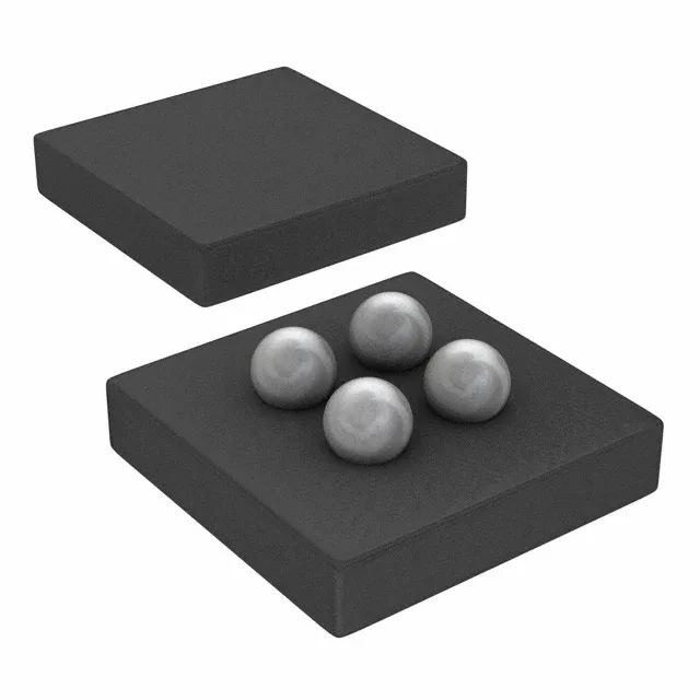
The CSD13302W: The 17.1 mOhm maximum on-resistance at 4.5 V gate drive sets the conduction loss floor for battery-powered rail switching or load-switch applications. The 4-DSBGA package measures 1x1 mm — roughly the footprint of a 0402 resistor. That shrinks the board area to almost nothing, but it also means the copper pad on the PCB is the primary heat path. The 1.8 W power dissipation rating at 25°C ambient assumes a standard footprint; in a tight layout with limited copper, the real thermal limit will be lower.
Gate charge is 7.8 nC at 4.5 V. The 862 pF input capacitance at 6 V Vds gives a rough handle on the Miller plateau. The 1.3 V maximum gate threshold at 250 µA means the FET is fully enhanced well below 2.5 V gate drive.
If dual-sourcing is critical, a larger-package alternative in the same voltage/current class (e.g. SOT-23) would require a board spin.
Temperature range and the 1x1 mm package — what the repair bench sees
The catch is the package: 4-DSBGA with no visible leads. On the repair bench, that means the scorch mark is the only clue the FET failed — you cannot probe the gate pad without a microprobe station. Rework requires hot air and a steady hand; the 1x1 mm body lifts easily if the board is not preheated.