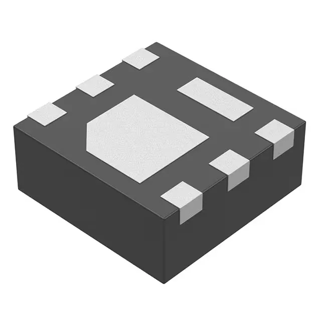
What this 12V NexFET does on the board
With a maximum Rds(on) of 9.3 mOhm at 4.5 V gate drive and 5 A drain current, this part is built for low-voltage, high-efficiency switching — think point-of-load converters, load switches, and battery protection in portable or embedded systems.
On-resistance and gate charge — the efficiency pair
The 9.3 mOhm Rds(on) at 4.5 V gate drive means conduction losses stay low even at several amps of load current. That 4.5 V drive level is important: it lets a 5 V rail or a 3.3 V system with a gate-drive booster turn the FET fully on without needing a 10 V supply. Gate charge is 6.6 nC at 4.5 V. For higher-frequency DC-DC converters, the low Qg keeps driver losses in check.
It is at home in outdoor telecom gear, engine-bay electronics, industrial motor drives, and battery packs that see thermal cycling. Maximum power dissipation is 2.7 W at 25°C ambient.