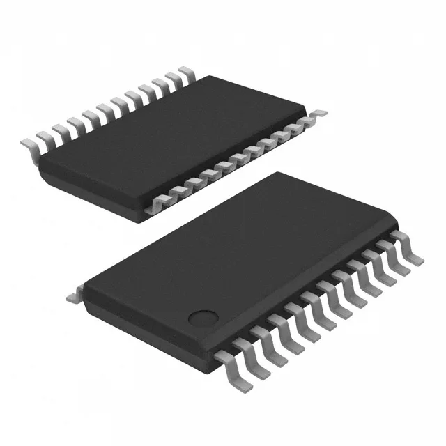
Texas Instruments CDCVF310PW — Clock & Timing ICs

CDCVF310PW Fanout Buffer, 1:10, 200 MHz, 24-TSSOP

MPNCDCVF310PW
End of Life

Texas Instruments CDCVF310PW, Fanout Buffer (Distribution), 1:10 LVTTL, 200 MHz max, 2.3V–3.6V supply, -40°C to 85°C, 24-TSSOP package.

$5.92Ref. price · indicative, final on quote
Packaging24-TSSOP (0.173", 4.40mm Width)
StockContact for availability
MOQ1 pcs
  • 100% new & originalTraceable channels only — no refurbs, no pulls, no remarked parts.
  • Date & lot codes on quoteStated per line before you commit; label photos on request.
  • MSL-compliant ESD packingMoisture-sealed bags with indicator cards; reels photo-verified.
  • PayPal buyer protectionPay by T/T, PayPal or Payoneer — card payments covered end to end.

Specifications

CDCVF310PW Technical Specifications
ParameterValue
TypeFanout Buffer (Distribution)
Mounting typeSurface Mount
Voltage2.3V ~ 3.6V
Frequency200 MHz
Operating temperature-40°C ~ 85°C
InputLVTTL
OutputLVTTL
PackageTube
Case24-TSSOP (0.173\", 4.40mm Width)
Number of circuits1
Ratio - Input:Output1:10
Differential - Input:OutputNo/No

Product details

Clock fanout for single-ended LVTTL trees

The Texas Instruments CDCVF310PW is a 1:10 fanout buffer that takes one LVTTL clock input and distributes it to ten LVTTL outputs. It handles clock rates up to 200 MHz, which covers the majority of board-level synchronous interfaces — SPI, parallel memory busses, and FPGA reference clocks — without needing a reclocking PLL. The supply range from 2.3V to 3.6V lets it sit on either a 2.5V or 3.3V rail, so it can bridge voltage domains in mixed-supply designs. Rated for the industrial temperature span of -40°C to 85°C, it fits outdoor telecom cabinets, factory-floor controllers, and base-station line cards.

200 MHz ceiling — what it means for the clock tree

The 200 MHz maximum frequency is the practical limit for the output edge rate and propagation consistency. If your system's fastest clock runs at 150 MHz, this buffer has 25% headroom before the output jitter starts degrading. For a 100 MHz reference driving ten FPGA banks, the 1:10 ratio saves a second buffer stage. The non-differential I/O (No/No) means this part is for single-ended LVTTL paths only — if your design uses LVPECL or LVDS, you need a different buffer family like the CDCLVP1204.

Supply and temperature — where it fits on the board

The 2.3V to 3.6V supply range covers the common 2.5V and 3.3V logic rails. At 3.3V the LVTTL outputs swing rail-to-rail, which gives clean noise margins into standard CMOS inputs. The industrial temperature rating (-40°C to 85°C) is the baseline for most non-automotive embedded systems — outdoor telecom, industrial control, and test equipment. If your ambient hits 105°C, this part is not rated for that; look at a wider-temp variant. The 24-TSSOP package (4.40 mm body width) is a fine-pitch surface-mount footprint; the 0.65 mm lead pitch needs a standard SMD reflow profile, and the MSL rating on the reel label tells you the bake requirement before rework.

Active lifecycle — no redesign pressure

The CDCVF310PW carries an Active product status per the manufacturer's lifecycle record. For a BOM line, this removes the urgency to qualify a second source or stockpile for an EOL. The part is ROHS3 compliant, which covers the EU RoHS exemption list through 2024. No lead-free transition issues on the assembly line.

Sourcing posture — quoted to order

This part is sourced through independent distribution channels. For small quantities or prototype builds, the 24-TSSOP package is straightforward to hand-assemble with a hot-air station and fine-tipped iron.

Frequently asked questions

What is the maximum frequency output of CDCVF310PW?

The CDCVF310PW is rated for a maximum frequency of 200 MHz. This is the upper limit for the output clock rate; for reliable operation, the input clock should not exceed this value.

Can CDCVF310PW be used with a 3.3V supply?

Yes, the supply voltage range is 2.3V to 3.6V, so 3.3V is within the operating range. At 3.3V the LVTTL outputs swing rail-to-rail for clean noise margins into standard CMOS inputs.

Does CDCVF310PW have a direct replacement or equivalent?

The CDCLVP1204RGTR is a different part — it uses LVPECL outputs, handles differential inputs, and runs up to 2 GHz. It is not a pin-compatible or functional equivalent for a single-ended LVTTL 1:10 fanout buffer. No direct replacement is listed in the manufacturer's cross-reference for this order code.