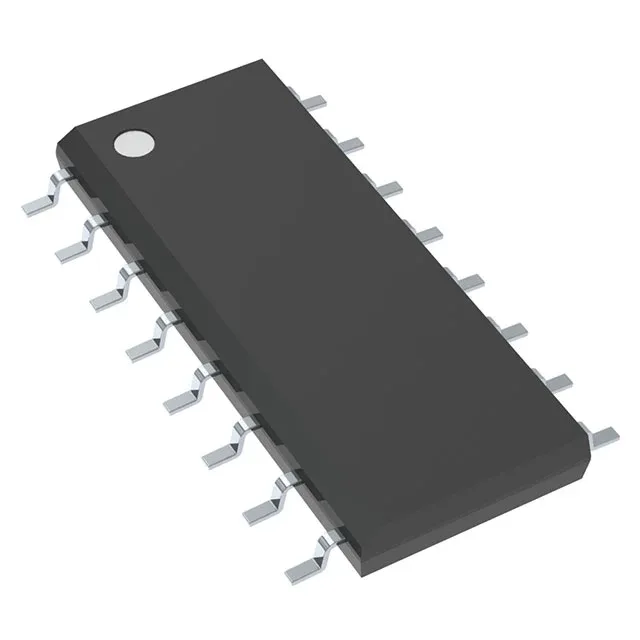
1:8 PLL clock driver for 3.3 V clock trees
The Texas Instruments CDCVF25081D is a single-circuit PLL clock driver with bypass, accepting two LVTTL inputs and delivering eight LVTTL outputs in a 16-SOIC package. It operates from a 3 V to 3.6 V supply and is rated for the industrial temperature range of -40°C to 85°C. The device is designed for clock distribution in systems where a clean, low-jitter clock is needed across multiple loads, such as networking equipment, base stations, and industrial controllers.
200 MHz maximum frequency — clock-tree headroom
The 200 MHz maximum frequency sets the upper bound for the output clock rate.
PLL with bypass — when to use each mode
The PLL includes a bypass mode. In normal operation, the PLL multiplies or cleans up the input clock, providing a frequency- and phase-locked output. In bypass mode, the input clock passes through to the outputs with minimal delay — essentially the device acts as a 1:8 fanout buffer. This is useful during system bring-up, for test modes, or when the input clock is already clean and only fanout is needed. The bypass feature means one BOM line item covers both use cases.
2:8 fanout — driving multiple loads from one device
With a 2:8 input-to-output ratio, the CDCVF25081D can distribute one or two clock sources to up to eight destinations.
For volume commitments or long-term BOM planning, no LTB risk is present.