Clock buffer with multiplier — what it does on your board
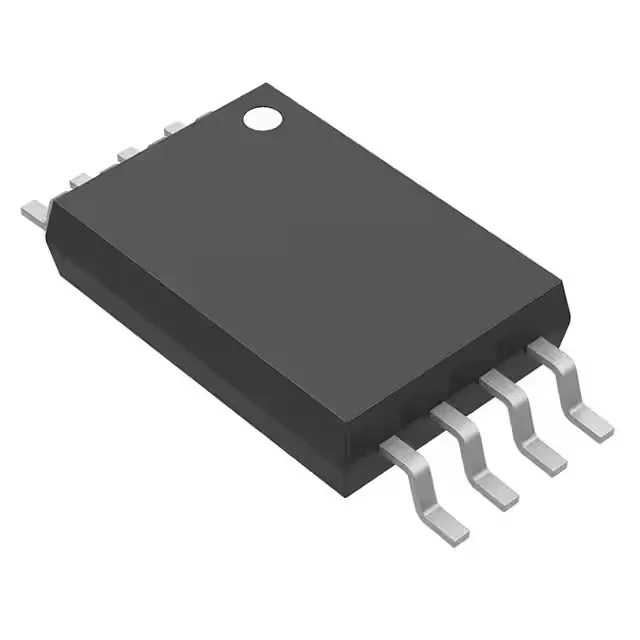
The Texas Instruments CDCS503PWR is a single-circuit LVCMOS clock buffer and multiplier in an 8-TSSOP package. It accepts one LVCMOS input and delivers one LVCMOS output at up to 108 MHz, with a 1:1 input-to-output ratio and no differential signalling on either side. The supply range is 3 V to 3.6 V, which means it runs cleanly off a standard 3.3 V rail but won't tolerate 2.5 V or 5 V without a regulator.
108 MHz max — what it means for clock-tree margin
The 108 MHz maximum frequency is the headline rating. In a typical clock-tree application you'd run it below that to leave margin for jitter and temperature drift — 80 to 90 MHz is a comfortable operating zone. Because it's a non-differential buffer (LVCMOS in, LVCMOS out), trace length matching matters less than it would for a LVPECL or LVDS fanout, but the single-ended output still needs a clean ground plane and a series termination resistor close to the pin to keep reflections off the clock line.