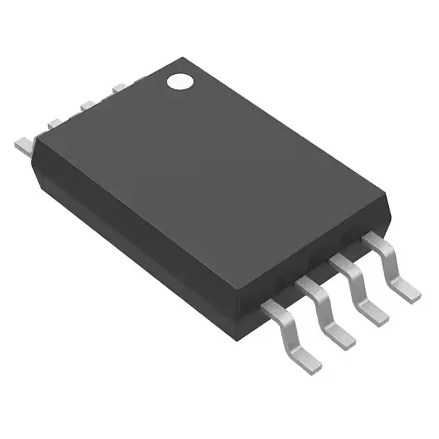
What this clock driver does for your board
The CDCS502PW is a Spread Spectrum Clock Driver — it takes a clean crystal input and modulates the output frequency slightly to spread the radiated energy, reducing EMI peaks that would otherwise fail FCC or CISPR limits. No PLL inside, so there is no frequency multiplication or phase locking; the output is a modulated version of the input, not a multiplied clock. Max output is 108 MHz, which covers most microcontroller, FPGA, and serial-interface reference clocks. Supply voltage is 3V to 3.6V — a tight 3.3V ±0.3V window. If your board already has a 3.3V rail, this part drops in. If you are running 5V or 1.8V logic, you need an additional regulator. The output is LVCMOS, so it drives standard CMOS inputs directly without level translation.
Suitable for outdoor telecom, motor drives, and factory automation where the ambient can swing. The 8-TSSOP package has a 4.40 mm body width and 0.65 mm pin pitch — a standard footprint that routes easily on two-layer boards. Surface-mount only. The 1:1 input-to-output ratio means one crystal drives one clock output. If you need to fan out to multiple loads, add a clock buffer after this device.
Production continues. No known successor or cross-reference from TI; this is the current-generation part. No stock-holding claim; we source per RFQ from our supply network.