Texas Instruments CDCP1803RGET — Clock & Timing ICs

CDCP1803RGET Clock Buffer 1:3 800MHz LVPECL 24-QFN

MPNCDCP1803RGET
End of Life

Texas Instruments CDCP1803RGET, Fanout Buffer (Distribution), Divider, Multiplexer, 1:3 ratio, 800 MHz max frequency, LVPECL output, 24-VFQFN Exposed Pad, -40°C to 85°C, Active

$8.81Ref. price · indicative, final on quote
Packaging24-VFQFN Exposed Pad
StockContact for availability
MOQ1 pcs
  • 100% new & originalTraceable channels only — no refurbs, no pulls, no remarked parts.
  • Date & lot codes on quoteStated per line before you commit; label photos on request.
  • MSL-compliant ESD packingMoisture-sealed bags with indicator cards; reels photo-verified.
  • PayPal buyer protectionPay by T/T, PayPal or Payoneer — card payments covered end to end.

Specifications

CDCP1803RGET Technical Specifications
ParameterValue
TypeFanout Buffer (Distribution), Divider, Multiplexer
Mounting typeSurface Mount
Voltage3V ~ 3.6V
Frequency800 MHz
Operating temperature-40°C ~ 85°C
InputCML, HSTL, LVCMOS, LVDS, LVTTL, SSTL-2, VML
OutputLVPECL
PackageTape & Reel (TR); Cut Tape (CT)
Case24-VFQFN Exposed Pad
Number of circuits1
Ratio - Input:Output1:3
Differential - Input:OutputYes/Yes

Product details

800 MHz LVPECL fanout with multi-standard input flexibility

The CDCP1803RGET is a 1:3 fanout buffer from Texas Instruments that accepts a wide range of input standards — CML, HSTL, LVCMOS, LVDS, LVTTL, SSTL-2, and VML — and delivers a single LVPECL output at frequencies up to 800 MHz. This input flexibility means the same part can sit behind a variety of clock sources without external level translators, simplifying the clock tree layout on mixed-signal boards.

Input-to-output mapping and differential path

The device provides a 1:3 ratio of differential inputs to differential outputs, with both input and output paths fully differential. This preserves signal integrity over the 800 MHz bandwidth, critical for jitter-sensitive applications like ADC sampling clocks or FPGA reference distribution.

Package and footprint considerations

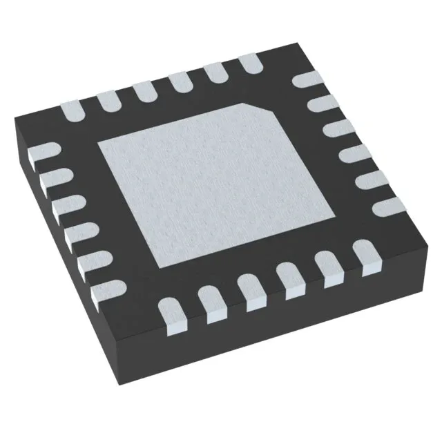
Housed in a 24-VFQFN with exposed pad (supplier package 24-VQFN, 4x4 mm). The 0.50 mm pitch QFN demands careful solder-paste stencil design and a controlled reflow profile to avoid bridging.

Lifecycle and sourcing posture

No end-of-life notification or successor has been issued. Standard TI distribution channels carry the part; procurement can be quoted against BOM quantities through our desk.

Frequently asked questions

Can CDCP1803RGET accept LVDS input and output LVPECL?

Yes. The input stage accepts LVDS (among other standards), and the output is LVPECL. The device performs the level translation internally, so no external resistor network or translator IC is needed between an LVDS oscillator and an LVPECL clock tree.

What is the closest functional second-source to CDCP1803RGET?

The CDCLVP1204RGTR is a peer from Texas Instruments with a 2:4 fanout ratio, LVPECL output, and a wider input range that includes LVCMOS, LVDS, LVPECL, and LVTTL. It operates up to 2 GHz and uses a 2.375 V supply. The CDCP1803RGET offers a 1:3 ratio and accepts additional input standards (CML, HSTL, SSTL-2, VML) at 3.0–3.6 V. They are not pin-compatible; evaluate the supply voltage and fanout count before cross-referencing.