What this part does in a high-speed clock tree
The Texas Instruments CDCM7005ZVA is a clock synchronizer and jitter cleaner built around a PLL with bypass capability. It accepts either single-ended LVCMOS or differential LVPECL reference inputs and delivers cleaned-up LVCMOS or LVPECL outputs at rates up to 1.5 GHz. The 3:10 input-to-output ratio gives you three reference inputs to select from and ten output copies, which is typical for fanning a recovered clock across multiple line-card ASICs or FPGAs.
1.5 GHz maximum frequency — sizing the PLL for your data rate
The 1.5 GHz maximum input frequency sets the upper bound for the reference clock. If you are clocking a 10 GbE PHY (156.25 MHz), a 12 Gbps SerDes (reference around 300–600 MHz), or a 100 GbE gearbox (multiple 644.53125 MHz references), this part has headroom. The PLL with bypass mode lets you either engage the loop for jitter attenuation or pass the reference straight through when the source is already clean — useful during system debug or when switching between a local oscillator and a recovered line clock.
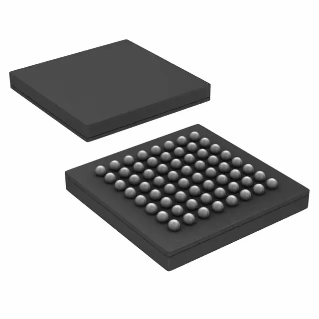
The 64-ball BGA (8x8 mm body) is a dense footprint — expect to route the LVPECL outputs as controlled-impedance differential pairs with proper AC-coupling if the receiver is CML or LVDS.