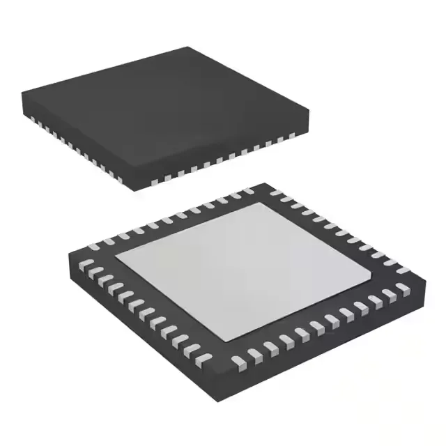
Texas Instruments CDCM7005RGZT — Clock & Timing ICs

CDCM7005RGZT Clock Synchronizer & Jitter Cleaner, 1.5 GHz

MPNCDCM7005RGZT
End of Life

Texas Instruments CDCM7005RGZT, Clock Synchronizer and Jitter Cleaner, PLL with Bypass, 1.5 GHz max, 3:10 LVCMOS/LVPECL I/O, 3V–3.6V supply, -40 to 85°C, 48-VQFN (7x7 mm), Surface Mount, ROHS3.

$21.38Ref. price · indicative, final on quote
Packaging48-VFQFN Exposed Pad
StockContact for availability
MOQ1 pcs
  • 100% new & originalTraceable channels only — no refurbs, no pulls, no remarked parts.
  • Date & lot codes on quoteStated per line before you commit; label photos on request.
  • MSL-compliant ESD packingMoisture-sealed bags with indicator cards; reels photo-verified.
  • PayPal buyer protectionPay by T/T, PayPal or Payoneer — card payments covered end to end.

Specifications

CDCM7005RGZT Technical Specifications
ParameterValue
TypeClock Synchronizer and Jitter Cleaner
Mounting typeSurface Mount
Voltage3V ~ 3.6V
Frequency1.5GHz
Operating temperature-40°C ~ 85°C
PLLYes with Bypass
InputLVCMOS, LVPECL
OutputLVCMOS, LVPECL
PackageTape & Reel (TR); Cut Tape (CT)
Case48-VFQFN Exposed Pad
Divider (Multiplier)Yes/No
Number of circuits1
Ratio - Input:Output3:10
Differential - Input:OutputYes/Yes

Product details

1.5 GHz clock synchronizer with jitter cleaning — what it does and where it fits

The Texas Instruments CDCM7005RGZT is a clock synchronizer and jitter cleaner built around a PLL that supports bypass mode. It accepts LVCMOS or LVPECL inputs and delivers LVCMOS or LVPECL outputs across a 3:10 input-to-output ratio, with a maximum operating frequency of 1.5 GHz. The part operates from a 3V to 3.6V supply and is rated over the -40°C to 85°C industrial temperature range, making it a fit for base stations, wireless infrastructure, and high-speed data converter clocking where phase noise and jitter budgets are tight.

PLL with bypass — why that matters for your clock tree

The PLL includes a bypass path, which means the device can pass a reference clock through without phase-locking when jitter cleaning is not needed. This is useful during system bring-up or when a clean external clock is already available. The differential input and output capability supports LVDS-like signalling for long PCB traces or backplane distribution, preserving signal integrity at 1.5 GHz.

Package and mounting — 48-VQFN with exposed pad

Housed in a 48-VQFN exposed-pad package measuring 7x7 mm. The exposed pad must be soldered to a thermal land on the PCB for adequate heat dissipation.

Lifecycle and sourcing posture

The CDCM7005RGZT carries an Active product status with ROHS3 compliance.

Frequently asked questions

What is the maximum frequency of CDCM7005RGZT?

The maximum frequency is 1.5 GHz, which covers high-speed serial clocking for gigabit transceivers, ADC/DAC sample clocks, and FPGA reference inputs.