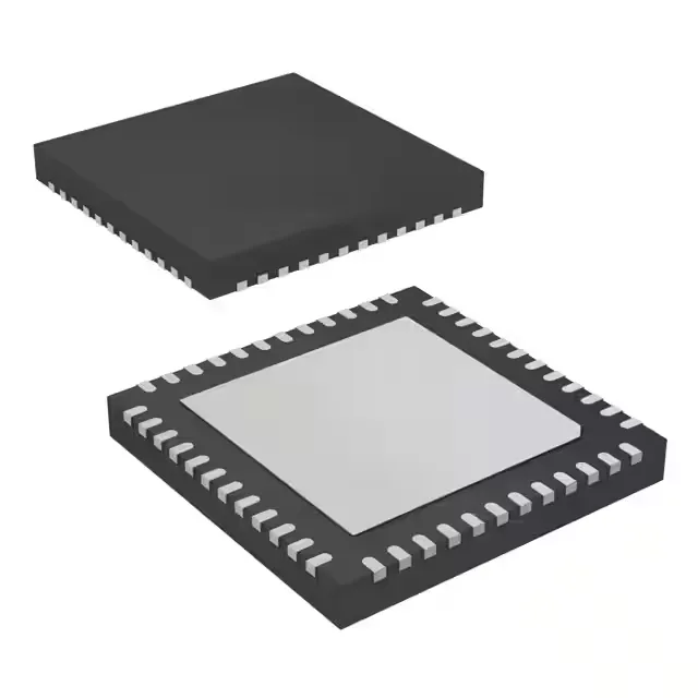
Texas Instruments CDCM6208V2RGZT — Clock & Timing ICs

CDCM6208V2RGZT Clock Generator, 800 MHz, 2:8 LVDS/PECL

MPNCDCM6208V2RGZT
End of Life

Texas Instruments CDCM6208V2RGZT, Clock Generator, PLL Yes with Bypass, 2:8 Input:Output, 800 MHz max, CML/HCSL/LVCMOS/LVDS/LVPECL I/O, 48-VQFN (7x7), -40°C to 85°C, ROHS3.

$13.45Ref. price · indicative, final on quote
Packaging48-VFQFN Exposed Pad
StockContact for availability
MOQ1 pcs
  • 100% new & originalTraceable channels only — no refurbs, no pulls, no remarked parts.
  • Date & lot codes on quoteStated per line before you commit; label photos on request.
  • MSL-compliant ESD packingMoisture-sealed bags with indicator cards; reels photo-verified.
  • PayPal buyer protectionPay by T/T, PayPal or Payoneer — card payments covered end to end.

Specifications

CDCM6208V2RGZT Technical Specifications
ParameterValue
TypeClock Generator
Mounting typeSurface Mount
Voltage1.71V ~ 3.465V
Frequency800MHz
Operating temperature-40°C ~ 85°C
PLLYes with Bypass
InputCML, LVCMOS, LVDS, LVPECL, Crystal
OutputCML, HCSL, LVCMOS, LVDS, LVPECL
PackageTape & Reel (TR); Cut Tape (CT)
Case48-VFQFN Exposed Pad
Divider (Multiplier)Yes/No
Number of circuits1
Ratio - Input:Output2:8
Differential - Input:OutputYes/Yes

Product details

What this clock generator does on your board

The Texas Instruments CDCM6208V2RGZT is a clock generator that takes up to two input references — CML, LVCMOS, LVDS, LVPECL, or a crystal — and produces eight output clocks in any combination of CML, HCSL, LVCMOS, LVDS, or LVPECL formats. The integrated PLL includes a bypass path, so the part can serve as either a jitter-cleaning frequency synthesizer or a low-skew fanout buffer depending on the signal integrity needs of the downstream SerDes, FPGA transceivers, or Ethernet PHYs. Maximum output frequency is 800 MHz. The 2:8 fanout ratio distributes a reference to eight destinations. Supply voltage spans 1.71 V to 3.465 V. Operating temperature range is -40°C to 85°C.

PLL with bypass — when to use which mode

The PLL includes a bypass mode. With the PLL engaged, the part cleans up jitter on the input reference and multiplies or divides to the target output frequency. In bypass mode, the input clock passes through to the outputs with minimal added phase noise — useful when the source is already clean and you only need fanout or format translation. The divider/multiplier path is available only when the PLL is active.

Signal format flexibility saves board space

Each of the eight outputs can be independently programmed to one of five differential or single-ended standards: CML, HCSL, LVCMOS, LVDS, or LVPECL. That means one clock generator can drive an FPGA bank expecting LVDS, a SerDes expecting CML, and a legacy ASIC expecting LVCMOS — all from the same device, no external level shifters or AC-coupling caps beyond what the standard itself requires. The differential input and output capability (Yes/Yes) means the part handles the full-speed differential paths that single-ended logic cannot maintain at 800 MHz without signal integrity problems.

Lifecycle and sourcing

The active status means no supply-risk premium for new designs.

Frequently asked questions

What is the maximum output frequency of CDCM6208V2RGZT?

The maximum output frequency is 800 MHz. This covers PCIe Gen 3/4 reference clocks, 10GbE, and common CPRI/OBSAI line rates.

Is CDCM6208V2RGZT compatible with LVDS inputs?

Yes, the part accepts LVDS inputs and can also output LVDS. The input accepts CML, LVCMOS, LVDS, LVPECL, or a crystal; the outputs can be independently configured to any of those formats plus HCSL.