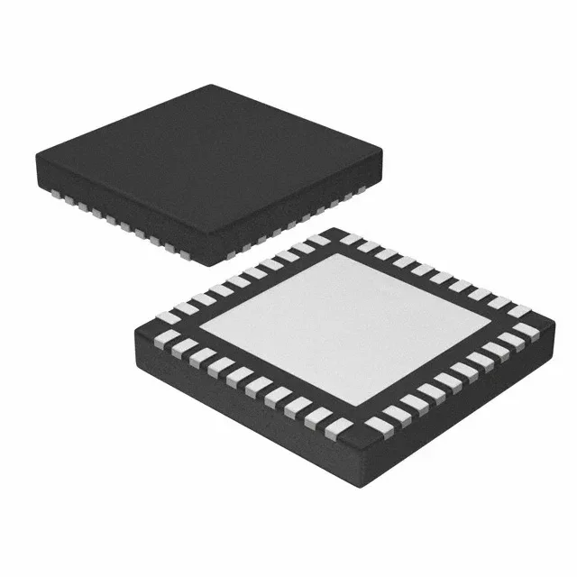
Texas Instruments CDCLVP1212RHAR — Clock & Timing ICs

CDCLVP1212RHAR Clock Buffer, 2:12 LVPECL Fanout, 2 GHz

MPNCDCLVP1212RHAR
End of Life

Texas Instruments CDCLVP1212RHAR, Fanout Buffer (Distribution), Multiplexer, 2:12 LVPECL output, 2 GHz max, LVCMOS/LVDS/LVPECL/LVTTL input, 2.375V-3.6V supply, -40°C to 85°C, 40-VQFN (6x6).

$15.27Ref. price · indicative, final on quote
Packaging40-VFQFN Exposed Pad
StockContact for availability
MOQ1 pcs
  • 100% new & originalTraceable channels only — no refurbs, no pulls, no remarked parts.
  • Date & lot codes on quoteStated per line before you commit; label photos on request.
  • MSL-compliant ESD packingMoisture-sealed bags with indicator cards; reels photo-verified.
  • PayPal buyer protectionPay by T/T, PayPal or Payoneer — card payments covered end to end.

Specifications

CDCLVP1212RHAR Technical Specifications
ParameterValue
TypeFanout Buffer (Distribution), Multiplexer
Mounting typeSurface Mount
Voltage2.375V ~ 3.6V
Frequency2 GHz
Operating temperature-40°C ~ 85°C
InputLVCMOS, LVDS, LVPECL, LVTTL
OutputLVPECL
PackageTape & Reel (TR); Cut Tape (CT)
Case40-VFQFN Exposed Pad
Number of circuits1
Ratio - Input:Output2:12
Differential - Input:OutputYes/Yes

Product details

What this clock buffer does on your board

The Texas Instruments CDCLVP1212RHAR is a 2:12 fanout buffer with an integrated 2:1 input multiplexer, designed to distribute one of two selectable clock sources to up to 12 LVPECL loads. It accepts LVCMOS, LVDS, LVPECL, or LVTTL inputs and outputs LVPECL, covering the common high-speed signaling standards used in telecom backplanes, data-center switches, and FPGA reference-clock trees. The part operates from a 2.375 V to 3.6 V supply and is rated for the industrial temperature range of -40°C to 85°C, making it suitable for outdoor base stations and factory-floor equipment where temperature swings are routine.

2 GHz bandwidth and 2:12 fanout — what they mean for your clock tree

The 2 GHz maximum frequency covers high-speed serial links. The 2:12 ratio means a single device replaces multiple lower-fanout buffers, saving board space and reducing part count. The differential input and output path preserves signal integrity over long traces.

Lifecycle and sourcing

The CDCLVP1212RHAR is listed as Active and ROHS3 compliant. There is no end-of-life notice or last-time-buy window to track. For current pricing and availability, submit an RFQ through the independent distribution channel — availability and pricing are confirmed at quote time. No immediate obsolescence risk; this part is still a valid choice for new production builds.

Frequently asked questions

What is the exact pinout of CDCLVP1212RHAR?

Designers need to validate PCB layout against the datasheet pin configuration.

Is CDCLVP1212RHAR an active or obsolete part?

Buyers and brokers need to know lifecycle status before ordering long-term.

What is the operating temperature range of CDCLVP1212RHAR?

Critical for determining if the part suits the intended environment.

What is the price for CDCLVP1212RHAR in quantities of 100?

Sourcing buyers need pricing to compare distributors and plan BOM costs.

Is CDCLVP1212RHAR available for immediate delivery?

Fast turnaround depends on stock availability from distributors.

What is the equivalent cross reference for CDCLVP1212RHAR?

Alternative parts may be needed for second sourcing or replacements.