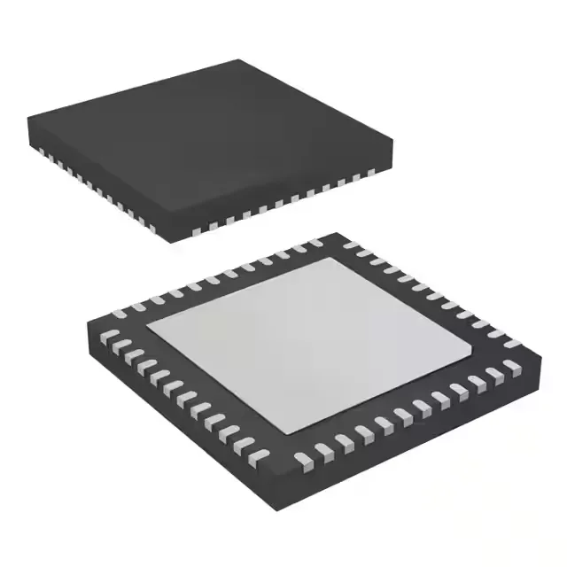
Clock fanout for high-speed backplanes and FPGA banks
The Texas Instruments CDCLVD2108RGZT is a fanout buffer that takes one clock input and delivers eight LVDS outputs across two independent buffer circuits. It accepts LVCMOS, LVDS, or LVPECL inputs and translates them to LVDS — a common requirement when a system clock source (crystal oscillator, PLL) needs to drive multiple FPGA transceiver banks, SerDes channels, or ADC/DAC clock inputs without degrading signal integrity. The 800 MHz maximum frequency covers most gigabit-class serial interfaces and high-speed memory buses.
Two independent 1:8 buffers — layout and fanout planning
With two circuits, each providing a 1:8 fanout, the part can distribute two separate clock domains from a single package — useful for splitting a reference clock and a data clock, or for driving separate FPGA banks with independent frequency/phase requirements. The 1:8 ratio per buffer means one input drives up to eight loads; plan the PCB trace length and impedance matching for LVDS routing to avoid skew across the fanout tree.
Input compatibility — LVCMOS, LVDS, LVPECL
The buffer accepts LVCMOS, LVDS, and LVPECL input levels, so it can sit behind a standard oscillator (LVCMOS), a differential PLL output (LVDS), or a legacy LVPECL clock source. The outputs are always LVDS, which is the dominant interface for high-speed clock distribution in modern digital systems. No external level translation is needed at the input — the buffer handles the conversion internally.