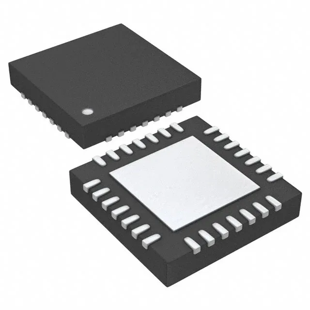
800 MHz fanout buffer with dual 1:4 trees
That means you can feed two separate clock domains from a single device, each getting a clean 1:4 split at up to 800 MHz. The differential input and output path is fully differential throughout, so common-mode noise on the clock line gets rejected rather than passed downstream.
Input flexibility saves a level translator
The input stage accepts LVCMOS single-ended signals as well as LVDS and LVPECL differential pairs. If your upstream oscillator or PLL puts out a 2.5V LVCMOS clock, you can feed it directly without an external level shifter — just one AC-coupling cap if the source is differential. The output is always LVDS, which is the standard for driving long PCB traces or backplane clock lines with low swing and good noise margin.
Industrial temperature range for outdoor and factory gear
The 2.375 V to 2.625 V supply rail is tight — 2.5 V nominal — so make sure your regulator holds within that window across load and temperature; a 3.3 V rail needs a separate 2.5 V LDO.
Package and layout: 28-VQFN with exposed pad
The pad is the main thermal path — without a via array under it, the junction temperature climbs fast if you run both circuits at full 800 MHz into 50-ohm loads. Keep the decoupling capacitors within 2 mm of the supply pins; the datasheet layout example is worth following closely.
It is RoHS3 compliant.