Texas Instruments CDCLVD1213RGTT — Clock & Timing ICs

CDCLVD1213RGTT Clock Buffer 1:4 800MHz LVDS – TI

MPNCDCLVD1213RGTT
End of Life

Texas Instruments CDCLVD1213RGTT, Fanout Buffer (Distribution), Divider, 1:4 LVDS output, 800 MHz max frequency, 2.375V–2.625V supply, 16-VQFN (3x3) exposed pad, -40°C to 85°C.

$11.19Ref. price · indicative, final on quote
Packaging16-VFQFN Exposed Pad
StockContact for availability
MOQ1 pcs
  • 100% new & originalTraceable channels only — no refurbs, no pulls, no remarked parts.
  • Date & lot codes on quoteStated per line before you commit; label photos on request.
  • MSL-compliant ESD packingMoisture-sealed bags with indicator cards; reels photo-verified.
  • PayPal buyer protectionPay by T/T, PayPal or Payoneer — card payments covered end to end.

Specifications

CDCLVD1213RGTT Technical Specifications
ParameterValue
TypeFanout Buffer (Distribution), Divider
Mounting typeSurface Mount
Voltage2.375V ~ 2.625V
Frequency800 MHz
Operating temperature-40°C ~ 85°C
InputCML, LVDS, LVPECL
OutputLVDS
PackageTape & Reel (TR); Cut Tape (CT)
Case16-VFQFN Exposed Pad
Number of circuits1
Ratio - Input:Output1:4
Differential - Input:OutputYes/Yes

Product details

1:4 LVDS fanout at 800 MHz – what it does

The CDCLVD1213RGTT is a single-channel fanout buffer that takes one differential input (CML, LVDS, or LVPECL) and distributes it to four LVDS outputs, with an optional divider stage. The 800 MHz maximum frequency covers common telecom and data-converter clock rates up to gigabit serial links. Supply voltage is 2.375V to 2.625V — a 2.5V rail with ±5% tolerance keeps the part in spec. The industrial temperature range suits base station, networking, and test equipment environments.

Input flexibility and output drive

Input accepts CML, LVDS, or LVPECL levels without external termination resistors for DC-coupled paths — the internal 100-Ω termination on the input pair handles the differential swing. Outputs are LVDS, which delivers 350 mV typical swing into a 100-Ω load, keeping EMI low on long backplane traces. The 1:4 fanout ratio means one clock source drives four receiver loads; the divider option lets you generate a sub-rate clock (e.g., half-frequency) from the same input. Both input and output paths are fully differential, so common-mode noise rejection is maintained through the buffer.

Package and footprint notes

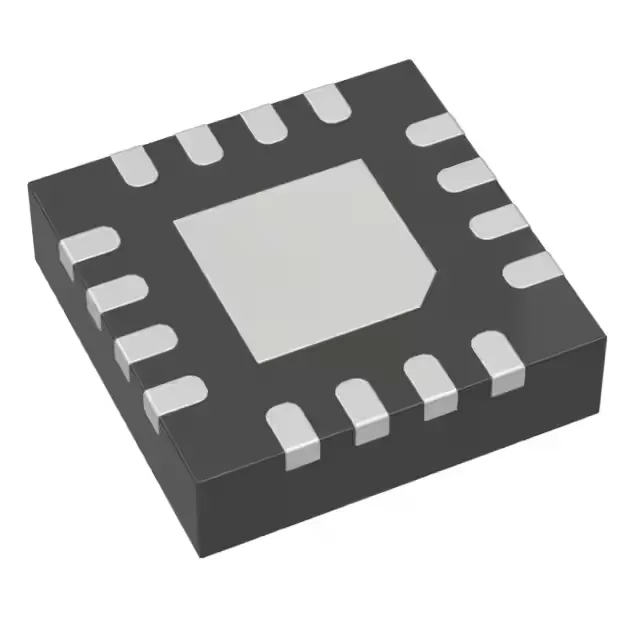
Housed in a 16-VFQFN with exposed pad, 3 mm × 3 mm body. Surface-mount with standard reflow profiles.

Production status and ordering

ROHS3 compliant. Sourced to order against BOM quantities. No firm stock or lead-time claim here — confirm availability and current pricing through an RFQ.

Frequently asked questions

What is the CDCLVD1213RGTT used for?

It distributes a high-speed clock or data signal to four LVDS destinations — common in FPGA reference clock trees, ADC/DAC clock distribution, and backplane timing for telecom and networking equipment. The divider option lets it generate a sub-rate clock from the same source.