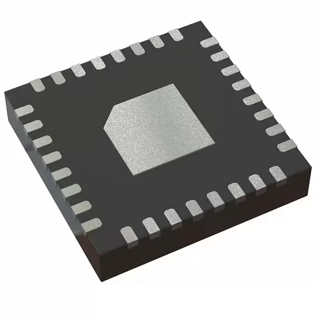
2:10 LVDS fanout at 1.1 GHz — what the ratio buys you
The CDCLVD110ARHBT is a 2:10 fanout buffer with an internal multiplexer, taking two LVDS inputs and distributing one selected clock to ten LVDS outputs at up to 1.1 GHz. The 2:10 ratio means you can feed two reference clocks and switch between them without an external mux — useful for redundant clock sources in base stations or test equipment where a single PLL feeds multiple ADC/DAC banks. All I/O are differential LVDS, so the part preserves signal integrity over longer board traces and through connectors compared to single-ended distribution. The differential input threshold is tight enough to accept a 100 mV swing, which keeps the buffer alive even with a degraded clock from a long backplane run.
Supply rail and temperature — the design-in constraints
The part runs on a single 2.5V supply with a tight tolerance of 2.375V to 2.625V. That narrow window means the 2.5V rail needs its own LDO or a clean switcher output — sharing a 3.3V rail with a buck regulator and dropping through a resistor divider will push the voltage out of spec under load. Plan for a dedicated 2.5V plane with local decoupling at the 32-VFQFN exposed pad. If your ambient hits 105°C, this part is not the right choice — look for a higher-temperature-grade LVDS buffer in the same family.
The exposed pad requires a solder paste stencil opening that matches the datasheet land pattern — a common layout gotcha that causes poor thermal contact and intermittent clock jitter.