1:10 LVCMOS fan-out at 250 MHz
The CDCLVC1110PWR is a single-channel fan-out buffer that takes one LVCMOS clock input and distributes it to ten LVCMOS outputs, rated up to 250 MHz. That 1:10 ratio means one oscillator or PLL source can feed ten loads — a typical FPGA bank, a set of ADCs, or a backplane clock tree — without needing a second buffer stage. Supply voltage spans 2.3V to 3.6V, so it runs directly off a 2.5V or 3.3V rail. No extra LDO or level shifter needed for the buffer itself, which saves board space and BOM cost.
Industrial temp and active production
Texas Instruments lists this part as Active. For ongoing builds, the supply chain is stable — no LTB window to manage, no forced last-time buy.
20-TSSOP package and board fit
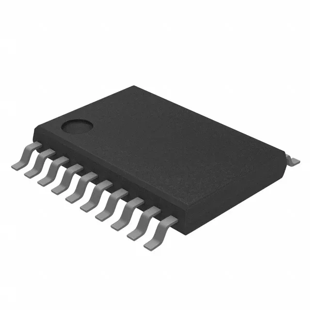
Housed in a 20-TSSOP (4.40 mm wide, 0.65 mm pitch), the CDCLVC1110PWR is a surface-mount part that routes easily on a two-layer board. The narrow body keeps the footprint small — useful when the buffer sits close to the clock source to minimise stub length.
Non-differential — LVCMOS only
The CDCLVC1110PWR is a non-differential buffer: both input and output are single-ended LVCMOS. If your design requires differential signalling (LVPECL, LVDS) or a 2:4 fan-out with a multiplexer, the CDCLVP1204RGTR is a different part — LVPECL outputs, 2 GHz max, 2:4 ratio, and differential inputs.