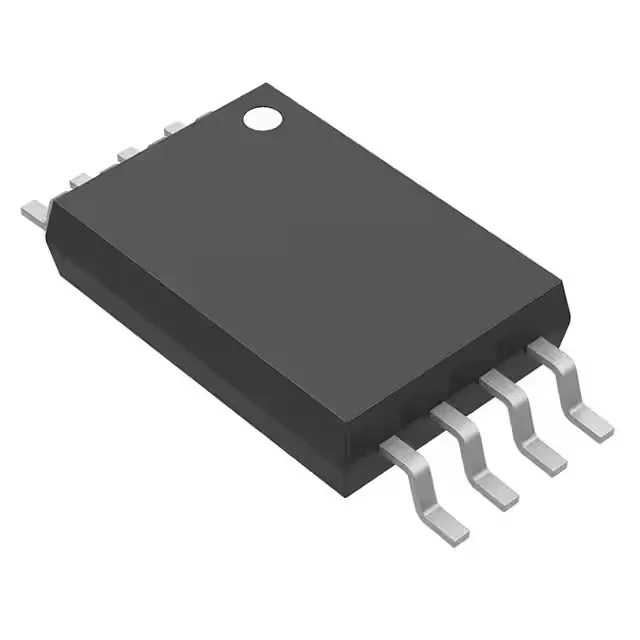
What this fanout buffer does on your clock tree
The CDCLVC1102PWR is a 1:2 fanout buffer that takes a single LVCMOS clock input and delivers two LVCMOS outputs with a maximum frequency of 250 MHz. The non-differential input and output architecture (No/No) means this part is intended for single-ended LVCMOS clock distribution, not for differential standards like LVPECL or LVDS.
250 MHz ceiling and the 1:2 ratio — fit for your system clock
At 250 MHz maximum frequency, this buffer can fan out a system clock up to that rate without adding jitter beyond the datasheet limits. The 1:2 ratio gives you two copies of the input clock — enough to drive two load points such as an FPGA and an Ethernet PHY from one source.