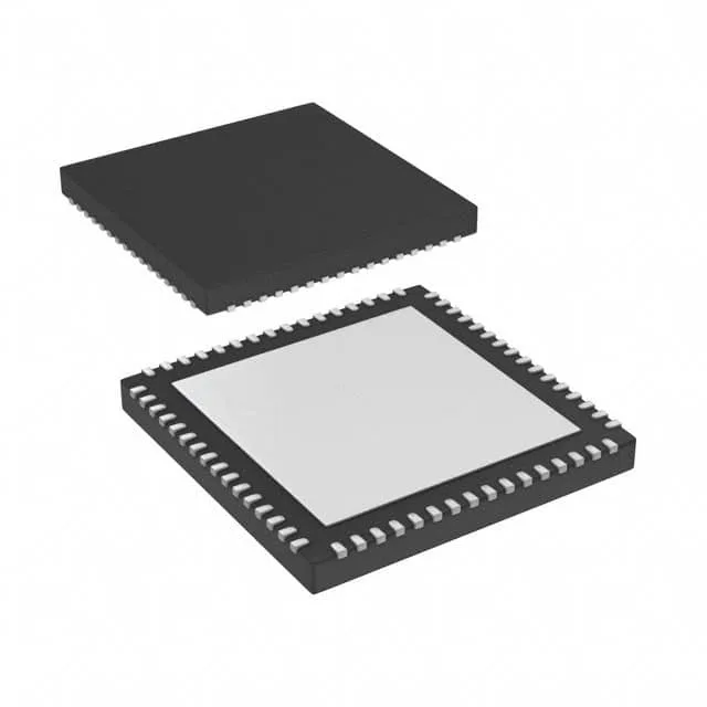
What this clock IC does and who needs it
The Texas Instruments CDCE72010RGCTG4 is a clock synchronizer, fanout distribution buffer, and jitter cleaner in one device — the kind of part a system architect reaches for when a board has multiple clock domains that must stay phase-aligned and low-noise. It integrates a PLL, accepts up to three reference inputs (LVCMOS, LVDS, or LVPECL), and drives up to twenty outputs in the same signal formats.
1.5 GHz ceiling and what it buys you
The maximum output frequency hits 1.5 GHz, which covers the fastest serial links in telecom backhaul, data converters, and FPGA transceiver reference clocks. At that speed, the PLL's jitter cleaning matters more than raw frequency — the part filters phase noise from a noisy VCXO or system clock before fanning it out to twenty destinations.
I/O flexibility saves board space
Both inputs and outputs support LVCMOS, LVDS, and LVPECL levels, so the same chip can bridge a single-ended reference to a differential clock tree or distribute LVPECL to multiple LVDS loads without external translators. The 3:20 ratio means one clean input can feed twenty receivers — useful when every FPGA or ADC on the board needs its own low-jitter clock.