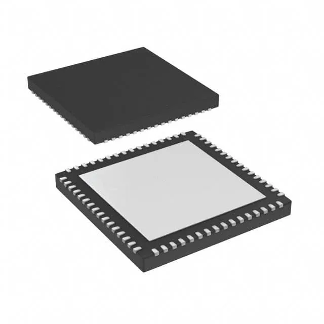
Texas Instruments CDCE72010RGCRG4 — Clock & Timing ICs

TI CDCE72010RGCRG4 Clock Synchronizer, 1.5 GHz PLL

MPNCDCE72010RGCRG4
End of Life

Texas Instruments CDCE72010RGCRG4, Clock Synchronizer, Fanout (Distribution), Jitter Cleaner, PLL, 1.5 GHz max frequency, 3:20 input:output ratio, LVCMOS/LVDS/LVPECL I/O, 3V~3.6V supply, -40°C~85°C, 64-VFQFN Exposed Pad.

StockContact for availability
MOQ1 pcs
  • 100% new & originalTraceable channels only — no refurbs, no pulls, no remarked parts.
  • Date & lot codes on quoteStated per line before you commit; label photos on request.
  • MSL-compliant ESD packingMoisture-sealed bags with indicator cards; reels photo-verified.
  • PayPal buyer protectionPay by T/T, PayPal or Payoneer — card payments covered end to end.

Specifications

CDCE72010RGCRG4 Technical Specifications
ParameterValue
TypeClock Synchronizer, Fanout (Distribution), Jitter Cleaner
Mounting typeSurface Mount
Voltage3V ~ 3.6V
Frequency1.5GHz
Operating temperature-40°C~85°C
PLLYes
InputLVCMOS, LVDS, LVPECL
OutputLVCMOS, LVDS, LVPECL
PackageTape & Reel (TR)
Case64-VFQFN Exposed Pad
Divider (Multiplier)Yes/No
Number of circuits1
Ratio - Input:Output3:20
Differential - Input:OutputYes/Yes

Product details

PLL clock conditioner with 1.5 GHz output ceiling

The Texas Instruments CDCE72010RGCRG4 is a PLL-based clock synchronizer, fanout buffer, and jitter cleaner that accepts up to three independent reference inputs (LVCMOS, LVDS, or LVPECL) and distributes them across twenty differential outputs running at up to 1.5 GHz. The 3:20 input-to-output ratio makes it a dense fanout solution for backplanes, wireless base station cards, and high-speed data converter clock trees where one device replaces multiple smaller fanout buffers.

TI lists the CDCE72010RGCRG4 with an active product status. For production builds that already qualify this device, the supply channel is stable through standard distribution and independent sourcing.

Differential I/O and 64-VFQFN footprint

All input and output paths support differential signalling (Yes/Yes in the differential I/O field), which is expected for a 1.5 GHz clock fanout — single-ended routing at that frequency would suffer excessive radiated emissions and skew.

Frequently asked questions

What voltage supply range does the CDCE72010RGCRG4 require?

All I/O banks and the PLL core share this rail, so a single 3.3 V output from a regulator or LDO is sufficient.

Can the CDCE72010RGCRG4 replace the base-number CDCE72010?

The CDCE72010RGCRG4 is a specific tape-and-reel variant of the base CDCE72010 device family. The RGCRG4 suffix indicates the 64-VFQFN package on tape-and-reel. Functionally it is the same die; the substitution depends only on whether the BOM specifies the reeled variant or a tube/tray version of the same package.