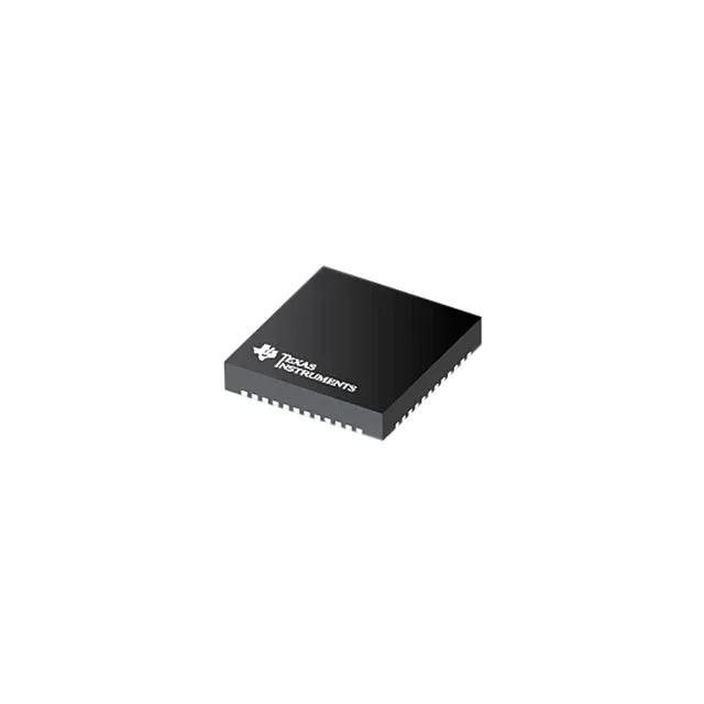
Texas Instruments CDCDB803RSLR — Clock & Timing ICs

CDCDB803RSLR Clock Buffer 1:8 250MHz 48VQFN - Texas

MPNCDCDB803RSLR
End of Life

Texas Instruments CDCDB803RSLR, Clock Buffer, 1:8 fanout, HCSL input and output, 250 MHz max frequency, 48-VFQFN exposed-pad package, -40°C to 105°C operation.

$4.92Ref. price · indicative, final on quote
Packaging48-VFQFN Exposed Pad
RoHSNot applicable
Independent supplier — new & surplus stockAuthenticity-screened · ESD-safe packingListing updated Aug 2026

Specifications

CDCDB803RSLR specifications
ParameterValue
TypeClock Buffer
MountingSurface Mount
Supply voltage3V ~ 3.6V
Frequency - max250 MHz
Operating temperature-40°C ~ 105°C (TA)
InputClock, HCSL
OutputClock, HCSL
PackageTape & Reel (TR); Cut Tape (CT)
Case48-VFQFN Exposed Pad
Number of circuits1
Ratio - Input:Output1:8
Differential - Input:OutputYes/Yes

Product details

250 MHz 1:8 HCSL fanout buffer

The CDCDB803RSLR is a 1:8 clock buffer from Texas Instruments that accepts one HCSL input and delivers eight HCSL outputs, each running up to 250 MHz. The differential HCSL signalling keeps edge rates clean for PCIe reference clocks, Ethernet PHY masters, and FPGA reference distribution.

The supply rail accepts 3V to 3.6V, so a nominal 3.3V rail with ±5% tolerance stays inside the window without an extra regulator.

48-VQFN package and reflow considerations

Standard lead-free reflow profile applies; no exotic process steps needed.

We source against your BOM quantity and confirm current pricing and lead time at quote — no stock-holding claim, no shelf-life risk.

Frequently asked questions

Is CDCDB803RSLR compatible with HCSL inputs?

Yes — the input stage is specified for HCSL (High-Speed Current Steering Logic) differential signals. The output also drives HCSL loads, so the entire fanout tree stays in the same logic family without level translation.