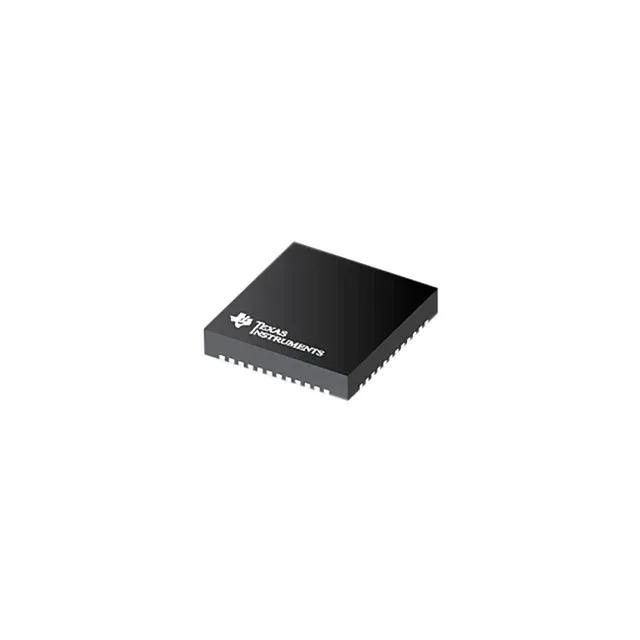
Texas Instruments CDCDB800RSLR — Clock & Timing ICs

CDCDB800RSLR Clock Buffer 1:8 250MHz 48VQFN Texas

MPNCDCDB800RSLR
End of Life

Texas Instruments CDCDB800RSLR, Clock Buffer, 1:8 fanout, 250 MHz max frequency, HCSL input/output, differential signalling, 48-VFQFN Exposed Pad (6x6 mm), -40°C to 105°C industrial temp range.

$4.92Ref. price · indicative, final on quote
Packaging48-VFQFN Exposed Pad
StockContact for availability
MOQ1 pcs
  • 100% new & originalTraceable channels only — no refurbs, no pulls, no remarked parts.
  • Date & lot codes on quoteStated per line before you commit; label photos on request.
  • MSL-compliant ESD packingMoisture-sealed bags with indicator cards; reels photo-verified.
  • PayPal buyer protectionPay by T/T, PayPal or Payoneer — card payments covered end to end.

Specifications

CDCDB800RSLR Technical Specifications
ParameterValue
TypeClock Buffer
Mounting typeSurface Mount
Voltage3V ~ 3.6V
Frequency250 MHz
Operating temperature-40°C ~ 105°C (TA)
InputClock, HCSL
OutputClock, HCSL
PackageTape & Reel (TR); Cut Tape (CT)
Case48-VFQFN Exposed Pad
Number of circuits1
Ratio - Input:Output1:8
Differential - Input:OutputYes/Yes

Product details

What this 1:8 HCSL buffer does for your clock tree

The CDCDB800RSLR is a 1:8 fanout clock buffer that accepts a single HCSL input and delivers eight HCSL outputs, each capable of 250 MHz. The differential HCSL signalling on both sides means it can distribute a clean PCIe or Ethernet reference clock over board traces without the common-mode noise pickup that plagues single-ended routing.

The 250 MHz max frequency sets the upper bound for the reference clock this buffer can pass without distortion. If your FPGA or SoC requires a 200 MHz or 156.25 MHz reference for 10GbE or PCIe Gen3, this part has headroom. The 1:8 ratio lets you drive multiple loads — eight SerDes transceivers, eight clocked ADCs, or a fan-out tree — from a single clean source, saving a secondary PLL or oscillator. Compared to the CDCLVP1204RGTR, which is a 2:4 LVPECL fanout buffer with a 2 GHz ceiling and a narrower -40°C to 85°C range, the CDCDB800RSLR trades top-end speed for wider temperature coverage and a larger fanout count (eight outputs vs four). The HCSL output type is also different — LVPECL requires DC-blocking caps and termination resistors that HCSL avoids, simplifying the BOM.

Active production — no immediate EOL concern

The 6x6 mm VQFN footprint is common enough that board layout guides and stencil apertures for the thermal pad are well-documented.

Frequently asked questions

Does the CDCDB800RSLR support 250 MHz operation?

Yes, the datasheet specifies a maximum frequency of 250 MHz. The input and output are both differential HCSL, which supports that speed with low jitter. For designs that need a 200 MHz or 156.25 MHz reference clock, this buffer has margin.