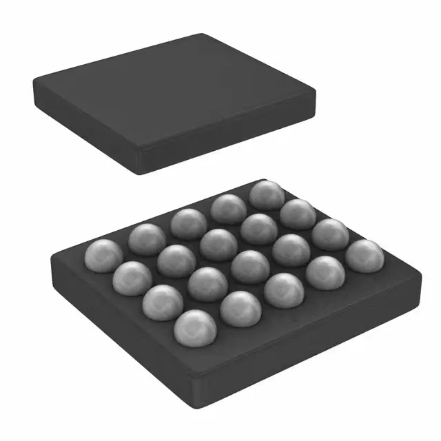
The CDC3S04YFFR is a single-ended 1:4 fanout buffer from Texas Instruments, designed to distribute a clock signal to up to four loads with minimal added jitter. It accepts a single clock input and outputs four identical clock copies, all within a 1.65V to 1.95V supply rail — common in 1.8V logic systems like FPGAs, MCUs, and SoCs that need a clean clock tree. Maximum frequency is 52 MHz, which covers most microcontroller and low-to-mid-range FPGA clock domains, but not high-speed serial links or RF sampling clocks. The non-differential I/O (single-ended only) means it's best suited for LVCMOS clock trees where skew and noise margin are managed by layout rather than differential routing.
The 1.65V to 1.95V supply range ties this buffer to low-voltage digital cores. If your system already has a 1.8V rail, this part drops in without an extra regulator. The 20-DSBGA package (0.4 mm pitch ball grid array) is compact — about 2.5 mm square — but requires a PCB with micro-vias or fine-trace fan-out. Hand-soldering is impractical; plan for a reflow profile and possibly a stencil. The small footprint saves board space in dense designs.