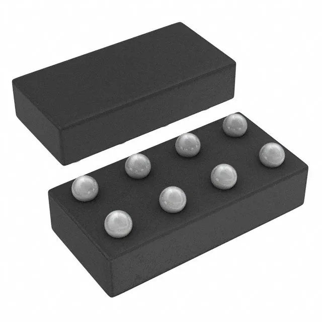
Texas Instruments CDC3RL02YFPR — Clock & Timing ICs

TI CDC3RL02YFPR Fanout Buffer, 52 MHz, 8-DSBGA

MPNCDC3RL02YFPR
End of Life

Texas Instruments CDC3RL02YFPR, Fanout Buffer (Distribution), 1:2 LVCMOS input/output, 52 MHz max, 2.3 V to 5.5 V supply, -40°C to 85°C, 8-DSBGA package.

$1.71Ref. price · indicative, final on quote
Packaging8-XFBGA, DSBGA
StockContact for availability
MOQ1 pcs
  • 100% new & originalTraceable channels only — no refurbs, no pulls, no remarked parts.
  • Date & lot codes on quoteStated per line before you commit; label photos on request.
  • MSL-compliant ESD packingMoisture-sealed bags with indicator cards; reels photo-verified.
  • PayPal buyer protectionPay by T/T, PayPal or Payoneer — card payments covered end to end.

Specifications

CDC3RL02YFPR Technical Specifications
ParameterValue
TypeFanout Buffer (Distribution)
Mounting typeSurface Mount
Voltage2.3V ~ 5.5V
Frequency52 MHz
Operating temperature-40°C ~ 85°C
InputLVCMOS
OutputLVCMOS
PackageTape & Reel (TR); Cut Tape (CT)
Case8-XFBGA, DSBGA
Number of circuits1
Ratio - Input:Output1:2
Differential - Input:OutputNo/No

Product details

1:2 LVCMOS fanout buffer for general-purpose clock distribution

The Texas Instruments CDC3RL02YFPR is a single-channel fanout buffer that distributes one LVCMOS input to two LVCMOS outputs. It operates from a 2.3 V to 5.5 V supply, making it suitable for mixed-voltage systems where a single buffer needs to bridge a 3.3 V clock source to a 5 V logic input or vice versa, as long as the levels are LVCMOS-compatible. The maximum output frequency is 52 MHz, which covers most microcontroller and FPGA reference clocks, SPI bus clocks, and general-purpose logic timing. The part is non-differential on both input and output (No/No), so it is strictly for single-ended LVCMOS clock trees. The industrial temperature range of -40°C to 85°C allows deployment in outdoor telecom cabinets, factory-floor controllers, and automotive cabin electronics that do not require AEC-Q100 qualification.

52 MHz ceiling and what it means for your clock tree

At 52 MHz, this buffer handles most common clock frequencies for 8-bit and 32-bit MCUs, audio codecs, and low-speed serial interfaces (I2C, SPI, UART). It is not intended for high-speed differential clocks (e.g., LVDS, LVPECL) or RF synthesizers. If your design requires fanout at 100 MHz or above, you would need a different buffer family such as the CDCLVP1204, which handles 2 GHz differential signals.

Package and footprint: 8-DSBGA

The 8-DSBGA package (0.4 mm pitch, 0.8 mm × 1.2 mm body) requires a fine-pitch PCB process. The landing pattern is non-standard for hobbyist boards; expect to use a 4-layer board with micro-vias if routing under the BGA. The part is surface-mount only, and the small footprint saves board area in space-constrained designs like handheld instruments or IoT modules.

Lifecycle and sourcing posture

The CDC3RL02YFPR is listed as Active by Texas Instruments, with ROHS3 compliance. This means it remains a safe choice for new production builds, and there is no last-time-buy pressure. For volume commitments, ask about lead time and factory order support.

Frequently asked questions

What is the supply voltage range of CDC3RL02YFPR?

Designers need to confirm compatibility with their system power rails.

Is CDC3RL02YFPR in stock at major distributors?

Buyers need availability to avoid production delays.

What is the price of CDC3RL02YFPR in 100-piece quantities?

Sourcing buyers require pricing for BOM costing.

Can CDC3RL02YFPR replace CDC3RL01?

Engineers and buyers often look for drop-in replacements to simplify redesign.

What is the output type of CDC3RL02YFPR?

Ensures the buffer drives downstream logic correctly (LVCMOS vs LVTTL).

Does CDC3RL02YFPR have any recommended alternative if obsolete?

Brokers and long‑term planners need lifecycle information for risk management.