The Texas Instruments CDC3RL02BYFPR is a 1:2 fanout buffer that takes a single LVCMOS clock input and delivers two LVCMOS outputs, rated for frequencies up to 52 MHz. It is not a PLL or jitter cleaner — it is a simple, low-skew distribution buffer for splitting a clock signal to two loads on the same board. The supply range from 2.3 V to 5.5 V means it can sit on a 3.3 V or 5 V rail without an extra regulator, and the industrial temperature grade (-40°C to 85°C) qualifies it for outdoor telecom cabinets, factory-floor controllers, and motor-drive control logic where the ambient sees thermal cycling.
The 52 MHz ceiling places this buffer in the low-to-mid-speed clock distribution tier. It handles the common 25 MHz, 40 MHz, and 50 MHz reference clocks used by MCUs, Ethernet PHYs, and FPGAs in the sub-100 MHz range. If your design distributes a 100 MHz+ oscillator or a high-speed serial reference, this part will not pass it — that is where a differential buffer like the CDCLVP1204 (2 GHz capable) would be needed. For a 50 MHz crystal oscillator feeding two downstream devices, the CDC3RL02BYFPR is a clean, low-cost fit.
Package and layout: 8-DSBGA
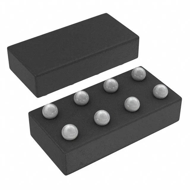
The 8-DSBGA package (0.4 mm pitch, roughly 1.6 mm × 1.6 mm body) is a tiny wafer-level chip-scale package. A solder-mask-defined pad with micro-vias under the BGA is the standard approach. No thermal pad to worry about; the package dissipation is low for a fanout buffer running at 52 MHz.