PLL clock distribution for 3.3V logic trees
It operates from a 3V to 3.6V supply — nominally 3.3V — and includes a PLL bypass mode that lets you feed the input straight through for test or low-jitter paths. Maximum output frequency is 125 MHz, which covers most DDR, PCI, and gigabit Ethernet reference clock trees in commercial equipment.
What the 1:16 fanout and 125 MHz ceiling mean for the BOM
The 125 MHz maximum frequency sets the upper bound.
Package and footprint — 48-TSSOP, 6.10 mm body
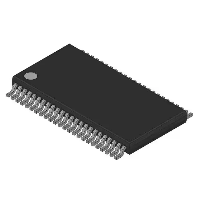
The CDC2516DGGR comes in a 48-lead TFSOP with a 6.10 mm body width. It is surface-mount only.
Both are the same silicon, so a BOM can accept either with a packaging note.