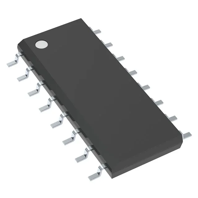
The 3-state outputs allow multiple devices to share a common bus line by placing outputs in a high-impedance state when the output-enable pins are asserted.
Supply rail and temperature — the two specs that decide fit
The supply range is strictly 4.5V to 5.5V — this is a 5V-only part, not a wide-range 2V-to-6V HC or HCT variant. If your board has a 3.3V logic rail, this buffer will not run from it. That temperature rating is the main reason to pick this over a commercial-grade 74HCT buffer: it keeps working in engine bays, cold-soaked outdoor cabinets, and high-altitude environments where a 0°C to 70°C part would fail.
Bus interface: 3-state and inverting logic
The CD74HCT368MT contains two elements: one 2-bit inverting buffer and one 4-bit inverting buffer, each with its own active-low output-enable pin. When the output-enable pin is high, the corresponding outputs go to high-impedance (Hi-Z), allowing other devices to drive the bus. This is a standard bus-interface function for address/data lines, control signals, or any shared-wire topology where contention must be avoided. The inverting nature means the output is the logical complement of the input — factor that into your signal polarity planning.
The mounting type is surface mount. For the PCB layout engineer: the standard SOIC-16 footprint applies; no thermal pad or exposed paddle is present.