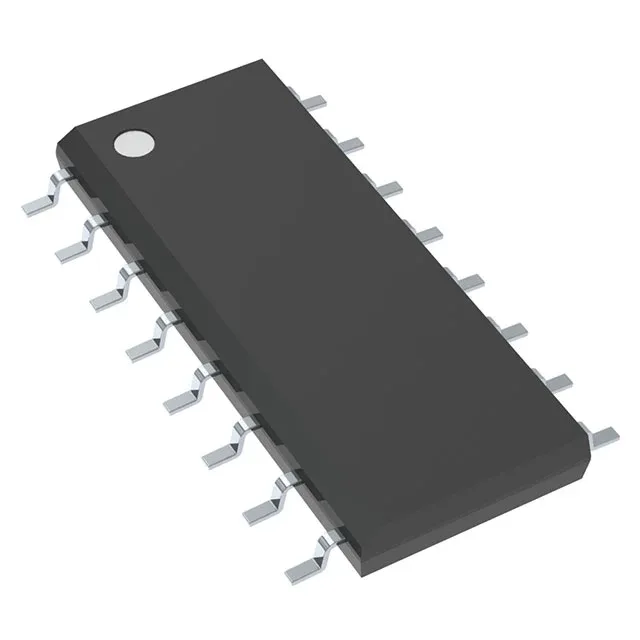
It selects one of eight data inputs and routes it to a single output, controlled by three address lines and an output-enable (strobe) pin. The 2V to 6V supply range means it works in 5V TTL systems as well as 3.3V or battery-powered designs.
Supply voltage and logic-level fit
The CD74HC251MT runs from 2V to 6V, so it is fully compatible with 5V logic — no level-shifting needed when interfacing with 5V microcontrollers or legacy TTL buses. At 5V the HC family's input thresholds are well within standard CMOS and TTL levels. The same part also works at 3.3V for mixed-voltage designs, though output drive is reduced at lower supply. The single-supply operation keeps the BOM simple — no separate analog rail needed.
The 74HC family is well-characterised over this range, so timing and drive strength are predictable. For a field-service swap, the 16-SOIC body is large enough to hand-solder with care, though a hot-air station is cleaner.
Output drive and fan-out
The CD74HC251MT can source or sink 5.2mA per output. That is typical for HC logic — enough to drive a few CMOS inputs, an LED with a series resistor, or a low-power relay driver through a transistor. For heavier loads, buffer the output. The output current is symmetric (5.2mA high, 5.2mA low), so the high and low levels have similar drive strength.
There is no announced end-of-life, so it is safe to qualify into new designs. No LTB risk or last-time-buy window to track.