What this buffer does that a standard op-amp can't
Its 3750V/µs slew rate and 210 MHz -3dB bandwidth put it in the class of parts you reach for when a standard op-amp's output stage can't drive a capacitive load or cable fast enough. The 250 mA output per channel means this isn't a signal-level part — it's meant to push video lines, drive ADC inputs through long traces, or buffer a reference into a heavy load.
A 3750V/µs slew rate means this buffer can swing a 10 V step in under 3 ns. That's the spec that tells you it's a high-speed part, not a general-purpose amplifier. For the repair bench or the design desk, the practical consequence is clean pulse response into loads that would slew-limit a 20 V/µs part into a triangle wave. The 210 MHz bandwidth supports video rates, fast pulse trains, and ADC front-end settling where the buffer's own rise time doesn't become the bottleneck. The input bias current of 250 nA is not the ultra-low figure you'd want for a precision integrator, but that's not the job here — this is a current buffer, not a preamp.
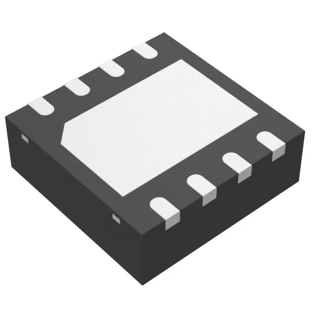
Surface-mount only; no through-hole variant in this order code.