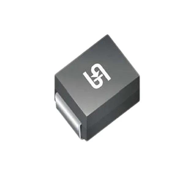
Clamping performance and peak-pulse energy
The 1.5SMC82CAHR7G: The 1.5 kW rating defines the transient energy the diode can absorb and safely shunt without degradation — critical for automotive ECU inputs and power-supply rails that face load-dump and inductive kickback transients. The bidirectional configuration means it clamps both polarities on the same two terminals, suitable for AC-coupled signal lines or where the protected node swings above and below ground.
The three-voltage window — standoff, breakdown, and clamping
Three voltage levels define the protection window. The reverse standoff voltage of 70.1 V is the maximum operating rail the TVS sees undisturbed in the off state — the line runs at or below this with only leakage current flowing. Minimum breakdown of 77.9 V marks where the avalanche mechanism engages and the diode begins conducting. The clamping voltage of 113 V is where the protected node is driven during a fault event; the downstream circuit must survive that clamped level, not the raw transient amplitude. Picking a TVS with the right standoff-to-clamping spread is the core design trade — tighter standoff gives lower leakage in normal operation but demands the downstream IC tolerates a higher clamped surge.
Automotive grade and thermal margin
AEC-Q101 qualification places this in the automotive discrete-semiconductor reliability stress set — the same temperature cycling, humidity, and surge-life screening applied to MOSFETs and rectifiers on the same BOM. Junction temperature range is -55 to 150 °C, covering under-hood ambient bands. Peak pulse rating is specified at 25 °C lead temperature; the 150 °C TJ ceiling sets the derating endpoint — above that the diode's ability to absorb transient energy drops per the normalised temperature curve in the datasheet.