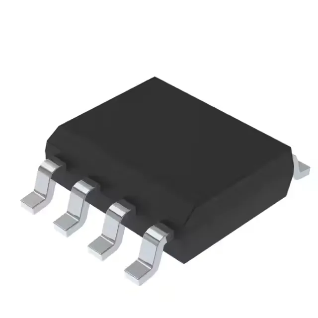
Current-mode PWM controller for boost and flyback converters
The STMicroelectronics UC2842BD1 is a current-mode PWM controller designed for step-up (boost) and flyback topologies, with a single transistor-driver output that switches an external MOSFET. It is a member of the UC2842 family, optimized for isolated and non-isolated DC-DC converters in industrial power supplies. The controller operates from a 10 V to 30 V supply rail and delivers a maximum duty cycle of 96%, which allows the output voltage to be regulated well above the input in boost or flyback configurations. The switching frequency reaches up to 500 kHz, enabling smaller magnetic components at the cost of higher switching losses in the external FET. The part is rated for an ambient temperature range of -25°C to +85°C, which covers most industrial and telecom indoor environments but not extended automotive or military temperature extremes.
Switching frequency and duty cycle trade-offs
With a switching frequency adjustable up to 500 kHz, the UC2842BD1 lets the designer shrink the transformer or inductor core size and reduce output capacitor ripple current. The trade-off is that gate-drive losses in the external MOSFET increase linearly with frequency — at 500 kHz the gate charge per cycle becomes a significant fraction of the total power budget. The 96% maximum duty cycle is critical for boost converters that need a high step-up ratio — for a 12 V input, the output can theoretically reach 288 V before the controller runs out of on-time. In practice, the transformer turns ratio and the MOSFET's drain-source breakdown voltage set the real limit. The controller includes frequency-control and positive-output-configuration features, and it is isolation-capable — meaning the feedback loop can cross a galvanic isolation barrier (typically via an optocoupler) for offline flyback supplies that must meet safety standards like IEC 60950.
Package and board-fit for the 8-SOIC footprint
The UC2842BD1 is supplied in an 8-SOIC package (3.90 mm body width) on tube. The surface-mount footprint matches the standard JEDEC MS-012 variation, with a 1.27 mm lead pitch. The package does not have an exposed thermal pad, so heat from the controller's internal circuitry must be conducted through the leads and the PCB copper to the ambient. For a typical flyback converter running at 100 kHz with a 12 V input and 5 V/2 A output, the controller's own dissipation is well under 0.5 W — the 8-SOIC's thermal impedance (junction-to-ambient around 120 °C/W) is adequate without forced airflow.