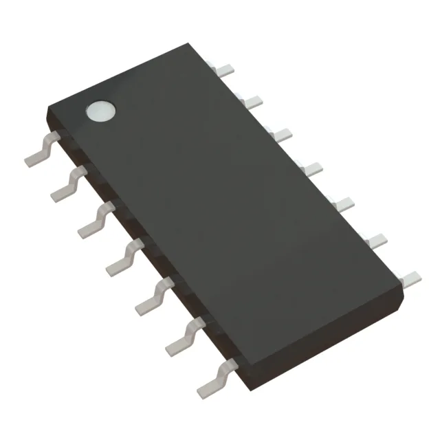
STMicroelectronics TSV914IYDT — Discrete Semiconductors

ST TSV914IYDT Op-Amp, 8 MHz, Automotive, 14-SOIC

MPNTSV914IYDT
End of Life

STMicroelectronics TSV914IYDT quad general-purpose op-amp, 8 MHz gain-bandwidth, 4.5 V/µs slew rate, rail-to-rail output, AEC-Q100 automotive grade, 14-SOIC package.

$2.14Ref. price · indicative, final on quote
Packaging14-SOIC (0.154", 3.90mm Width)
RoHSROHS3 Compliant
Independent supplier — new & surplus stockAuthenticity-screened · ESD-safe packingListing updated Aug 2026

Specifications

TSV914IYDT specifications
ParameterValue
Output typeRail-to-Rail
MountingSurface Mount
Amplifier typeGeneral Purpose
Voltage - input offset100 µV
Voltage - supply span5.5 V
Current - supply780µA (x4 Channels)
Current - input bias1 pA
Current - output (Channel)35 mA
Operating temperature-40°C ~ 125°C
Gain bandwidth product8 MHz
GradeAutomotive
PackageTape & Reel (TR); Cut Tape (CT)
Slew rate4.5V/µs
QualificationAEC-Q100
Case14-SOIC (0.154\", 3.90mm Width)
Number of circuits4

Product details

Automotive-grade quad op-amp for sensor conditioning and signal chains

The TSV914IYDT: Input bias current is 1 pA typical, so a high-impedance source like a piezo film or a pH electrode sees negligible loading. The 100 µV input offset is the dominant DC error term — budget it into the system accuracy calculation, especially if the signal chain has no auto-zero or chopper stage.

Package, pinout, and second-source fit

The supplier device package code 14-SO confirms it is the narrow-body variant — no footprint change from the industrial-grade TSV914IDT. The TSV914IDT (same pinout, same 8 MHz GBW, same 4.5 V/µs slew rate, same 1 pA input bias) is the closest functional equivalent. The only parametric difference is the input offset voltage: 100 µV for the IYDT vs 150 µV for the TSV914AIDT. A board laid out for the TSV914IDT accepts the TSV914IYDT without rewiring — the pin 1 orientation and pad geometry are identical.

Lifecycle, compliance, and sourcing note

The part is not single-sourced — the TSV914IDT provides a pin-compatible second-source path with the same package and parametric envelope.

Frequently asked questions

Will the TSV914IYDT drop into a board designed for the TSV914IDT?

Yes. Both parts share the same 14-SOIC package (0.154-inch body width), the same pinout, and the same 8 MHz gain-bandwidth product and 4.5 V/µs slew rate. The only difference is the input offset voltage grade — 100 µV for the IYDT vs 150 µV for the TSV914AIDT. No board spin or rewiring is required.

What compliance documentation does STMicroelectronics provide for the TSV914IYDT?

The part is ROHS3 compliant per STMicroelectronics' lifecycle record. No UL or IEC certification is listed in the available documentation. Standard STMicroelectronics material declaration and REACH reports are available through the distributor upon request.