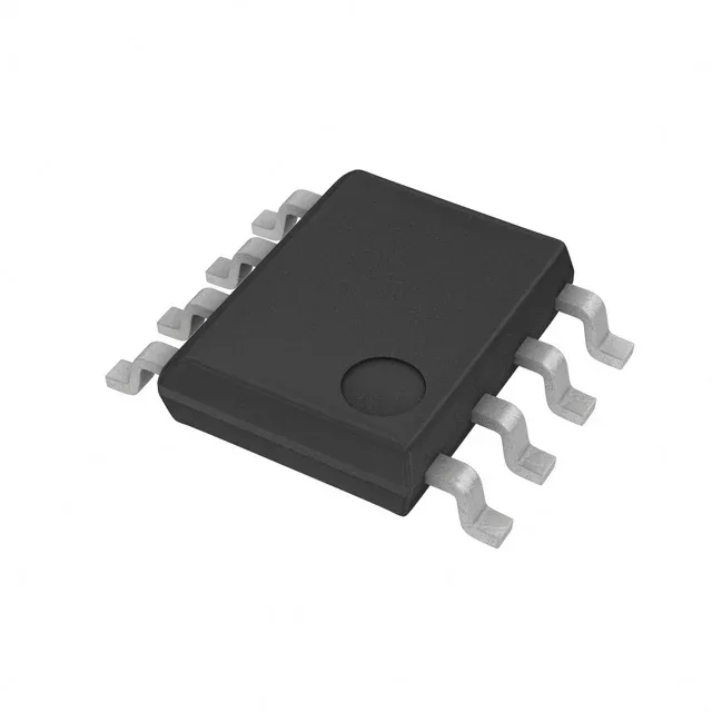
Active Automotive-Grade Dual Op Amp for Signal Conditioning
The TSV852IYST: With a gain-bandwidth product of 1.3 MHz and a 0.7 V/µs slew rate, it is sized for sensor signal conditioning, actuator feedback loops, and general-purpose analog processing in engine bay or cabin electronics where the temperature grade is the binding constraint.
Supply Rails and Output Drive for 5 V and 3.3 V Systems
Operating from a single supply span of 2.3 V to 5.5 V, the TSV852IYST covers the common automotive rail voltages — 3.3 V and 5 V — without needing a split supply. The rail-to-rail output stage swings within millivolts of both supply rails, preserving dynamic range at low supply voltages, and can source or sink 70 mA per channel — enough to drive an ADC input or a small relay coil directly. Total supply current is 130 µA per amplifier (260 µA for both channels), keeping the thermal budget low in dense PCB layouts.
Package and Footprint — 8-MiniSO for Space-Constrained Boards
Housed in the 8-MiniSO package (3.00 mm × 4.90 mm body, 0.65 mm pitch), the TSV852IYST fits into the same land pattern as a standard 8-TSSOP or 8-MSOP — no board respin needed if migrating from a similar footprint. The surface-mount package is supplied on tape and reel (TR) or cut tape (CT), compatible with standard pick-and-place and reflow profiles for MSL-1 or MSL-2 moisture sensitivity levels typical of MiniSO packages.
Input Offset and Bias — What the Numbers Mean for DC Accuracy
Maximum input offset voltage is 4 mV — this is the worst-case DC error at the output after the closed-loop gain. For a gain-of-10 stage, the output offset is up to 40 mV; if the downstream ADC has a 0 V to 5 V input range, that offset consumes roughly 0.8% of the span. Input bias current is 27 nA typical — negligible when driving a 10 kΩ source impedance (creates 270 µV of additional offset), but significant with a 1 MΩ source (27 mV drop). For high-impedance sensors, use the TSV852IYST with source impedances below 100 kΩ to keep the bias-current error under 2.7 mV.