STMicroelectronics TSB582IQ2T — Logic ICs

STMicro TSB582IQ2T CMOS Op-Amp, 3.1 MHz, 200 mA Output

MPNTSB582IQ2T
End of Life

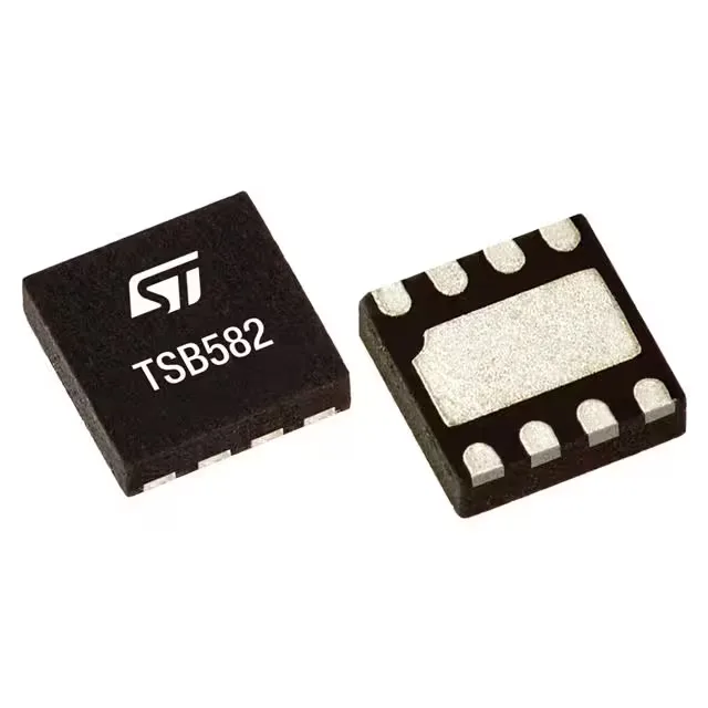
STMicroelectronics TSB582IQ2T dual CMOS operational amplifier, 3.1 MHz gain bandwidth, 2 V/µs slew rate, rail-to-rail output, 200 mA output per channel, 2 V to 36 V supply, -40 to 125°C, 8-DFN exposed pad.

$3.79Ref. price · indicative, final on quote
Packaging8-WDFN Exposed Pad
StockContact for availability
MOQ1 pcs
  • 100% new & originalTraceable channels only — no refurbs, no pulls, no remarked parts.
  • Date & lot codes on quoteStated per line before you commit; label photos on request.
  • MSL-compliant ESD packingMoisture-sealed bags with indicator cards; reels photo-verified.
  • PayPal buyer protectionPay by T/T, PayPal or Payoneer — card payments covered end to end.

Specifications

TSB582IQ2T Technical Specifications
ParameterValue
Output typeRail-to-Rail
Mounting typeSurface Mount
Amplifier typeCMOS
Voltage - input offset2.4 mV
Voltage - supply span36 V
Current - supply2.5mA (x2 Channels)
Current - input bias2 nA
Current - output (Channel)200 mA
Operating temperature-40°C ~ 125°C
Gain bandwidth product3.1 MHz
PackageTape & Reel (TR); Cut Tape (CT)
Slew rate2V/µs
Case8-WDFN Exposed Pad
Number of circuits2

Product details

Dual CMOS op-amp with 200 mA output drive

The STMicroelectronics TSB582IQ2T is a dual CMOS operational amplifier that delivers a rare combination for a small-package op-amp: 200 mA of output current per channel from a rail-to-rail output stage. With a 3.1 MHz gain-bandwidth product and 2 V/µs slew rate, it handles sensor conditioning, actuator drive, and power-rail buffering in one device.

Most small CMOS op-amps top out at 20–50 mA output. The TSB582IQ2T's 200 mA per channel eliminates a separate buffer or transistor stage when driving a solenoid, a piezo actuator, or the feedback winding of a power converter. That saves board area and one or two BOM lines. The thermal protection built into the output stage (flagged in the description as 'HIGH OUTPUT CURRENT WITH THERMAL') means it survives a sustained short without self-destructing — useful in industrial modules where the load is hot-plugged.

Package and footprint reality

The 8-WDFN with exposed pad (3x3 mm body) is the only package option for this order code. This is a surface-mount part, so reflow profile follows standard lead-free (260°C peak) with MSL 3 moisture sensitivity.

Active status, no LTB risk

ROHS3 compliance is confirmed.

Frequently asked questions

Will TSB582IQ2T drop into a panel that was specified around TSB582IYQ2T without rewiring?

The TSB582IYQ2T is the automotive-grade (AEC-Q100) variant of the same base amplifier. Both share the same 3.1 MHz GBW, 2 V/µs slew rate, 200 mA output, and 8-DFN package. The TSB582IQ2T lacks the AEC-Q100 qualification but is otherwise pin-compatible and functionally identical. For a non-automotive panel it is a drop-in replacement; for automotive applications the IY suffix variant is required.