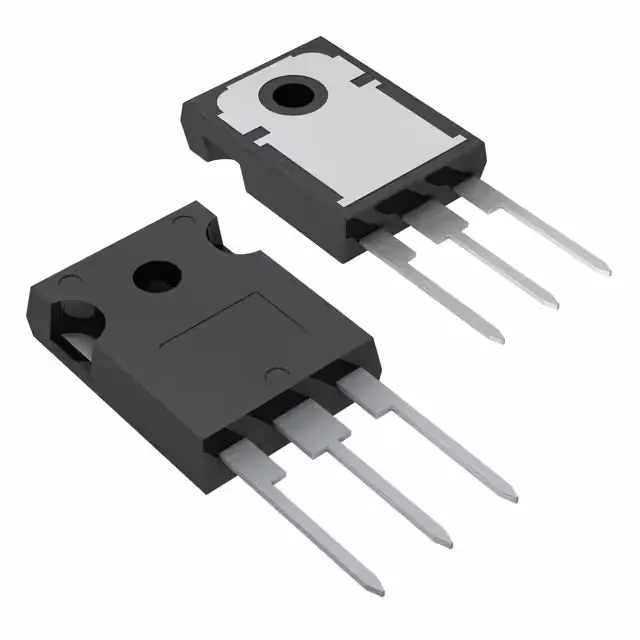
500 V N-channel MDmesh™ II MOSFET in TO-247-3
Gate charge totals 34 nC at 10 V, a figure that determines the driver's switching loss budget and the minimum drive current needed at the target frequency.
This is the value used for conduction loss calculation at full load; actual on-resistance rises with junction temperature, so the thermal design must account for the positive temperature coefficient typical of MDmesh™ II devices. Input capacitance is 1000 pF at 50 V drain-source, which together with the gate charge defines the driver's peak current requirement.
Housed in a TO-247-3 through-hole package, the STW19NM50N is designed for bolted mounting to a heatsink. The maximum power dissipation is 110 W at case temperature, making the thermal interface and heatsink selection the dominant factor in the junction temperature budget.