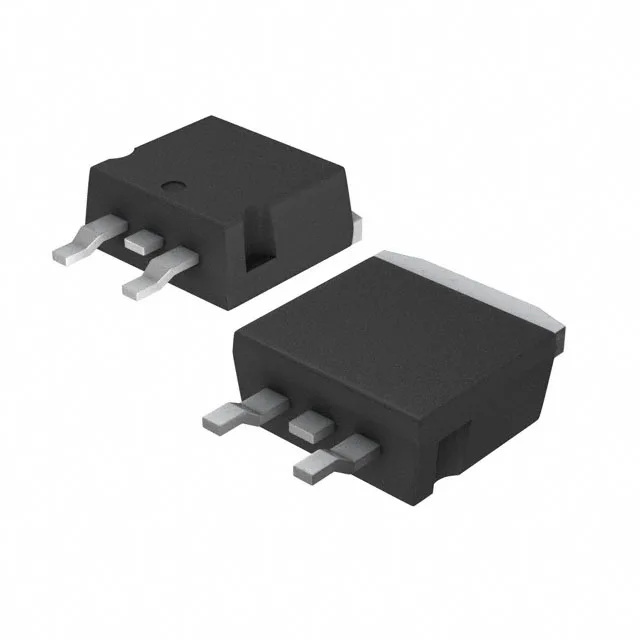
SiC Schottky — why the recovery time matters for the PFC stage
The STPSC8H065G-TR is a 650 V, 8 A silicon-carbide Schottky diode from STMicroelectronics, packaged in a D²PAK (TO-263) for surface-mount assembly. Its defining characteristic is zero reverse recovery time — the SiC Schottky barrier eliminates the stored-charge tail that forces every silicon ultrafast diode to burn switching energy at every turn-off. For a continuous-conduction-mode PFC boost stage, that zero trr directly cuts the MOSFET turn-on loss by the amount the silicon diode's reverse recovery would have cost.
650 V blocking and 8 A forward — sizing the power rail
The 650 V reverse voltage covers universal-input PFC stages (nominal 400 V DC bus) with margin for line transients. The 8 A average forward current supports output power levels around 300 W to 1.5 kW in a boost converter, depending on the topology and cooling. Forward voltage at the rated 8 A is 1.75 V maximum — that figure sets the conduction loss at full load and drives the D²PAK pad's thermal design. The 80 µA reverse leakage at 650 V is negligible at 25 °C but doubles roughly every 10 °C junction rise, so at 150 °C junction the leakage contribution to the standby budget needs a quick check.
D²PAK footprint — same land pattern as silicon ultrafast diodes
The TO-263-3 (D²PAK) package is the standard surface-mount power-diode footprint. The STPSC8H065G-TR uses the same 2-lead-plus-tab land pattern as common silicon ultrafast diodes in this current class — a direct drop-in replacement on the PCB layout, provided the gate-drive timing in the controller accounts for the zero trr.
STMicroelectronics lists the STPSC8H065G-TR as an active product.